Semiconductor Device, Module, and Electronic Device

a technology of semiconductors and semiconductor devices, applied in the direction of semiconductor devices, electrical apparatus, transistors, etc., can solve the problems of small power consumption of display devices in which a transistor including an oxide semiconductor is used, and achieve the effects of stable electrical characteristics, stable electrical characteristics, and stable electrical characteristics

Inactive Publication Date: 2016-06-02
SEMICON ENERGY LAB CO LTD
View PDF1 Cites 7 Cited by
  • Summary
  • Abstract
  • Description
  • Claims
  • Application Information

AI Technical Summary

Benefits of technology

[0010]An object is to provide an element with stable electrical characteristics. An object is to provide a device including plural kinds of elements with stable electrical characteristics. An object is to provide a transistor with stable electrical characteristics. Another object is to provide a transistor with normally-off electrical characteristics. Another object is to provide a transistor with a small subthreshold swing value. Another object is to provide a transistor having a small short-channel effect. Another object is to provide a transistor having a low leakage current in an off state. Another object is to provide a transistor with excellent electrical characteristics. Another object is to provide a highly reliable transistor. Another object is to provide a transistor with high frequency characteristics.

Problems solved by technology

For example, a display device in which a transistor including an oxide semiconductor is used is known to have small power consumption.

Method used


Image

  • Semiconductor Device, Module, and Electronic Device
  • Semiconductor Device, Module, and Electronic Device
  • Semiconductor Device, Module, and Electronic Device

Examples


Embodiment Construction

[0081]Hereinafter, embodiments and examples of the present invention will be described in detail with the reference to the drawings. However, the present invention is not limited to the description below, and it is easily understood by those skilled in the art that modes and details disclosed herein can be modified in various ways. Further, the present invention is not construed as being limited to description of the embodiments and the examples. In describing structures of the present invention with reference to the drawings, common reference numerals are used for the same portions in different drawings. Note that the same hatched pattern is applied to similar parts, and the similar parts are not especially denoted by reference numerals in some cases.

[0082]Note that the size, the thickness of films (layers), or regions in drawings is sometimes exaggerated for simplicity.

[0083]In this specification, the terms “film” and “layer” can be interchanged with each other.

[0084]A voltage usu...


PUM


Abstract

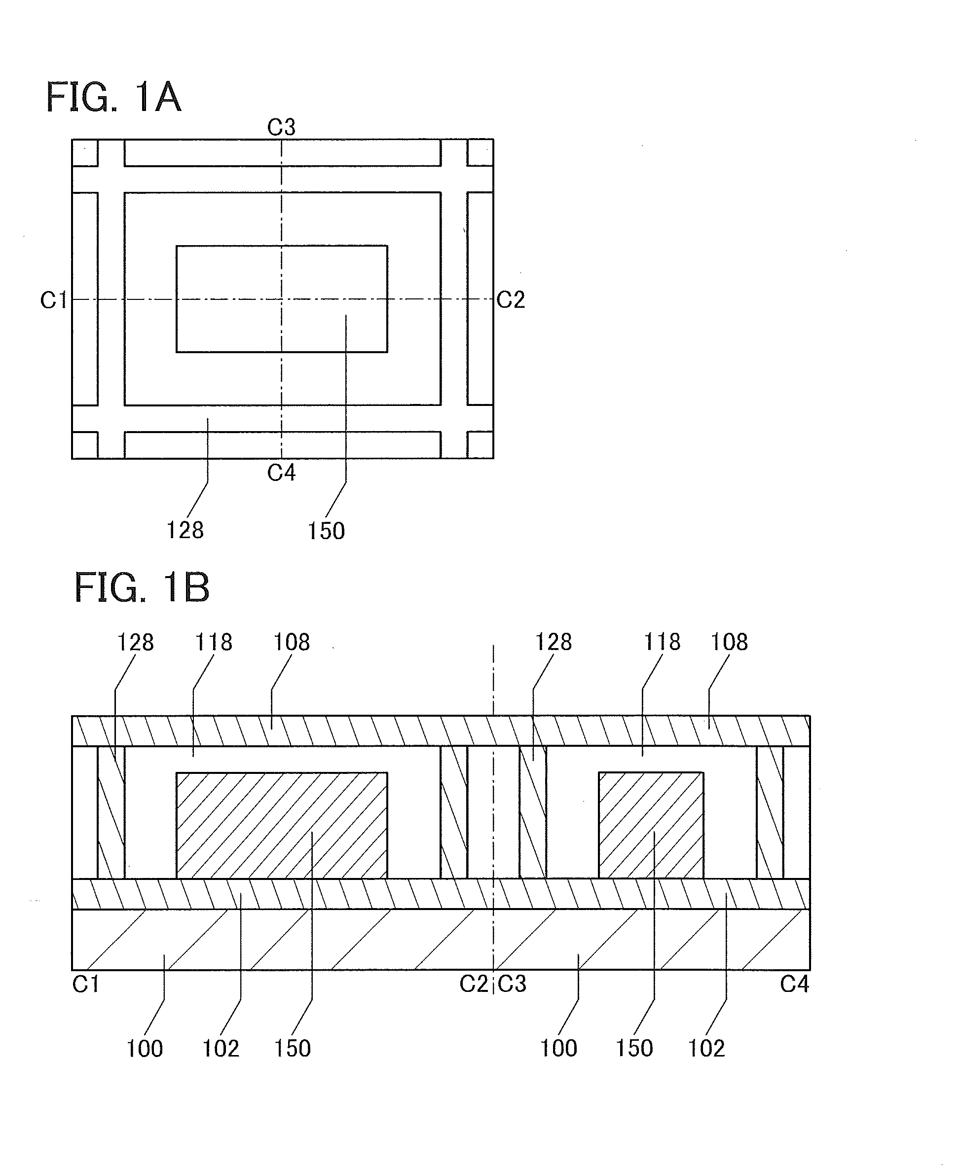
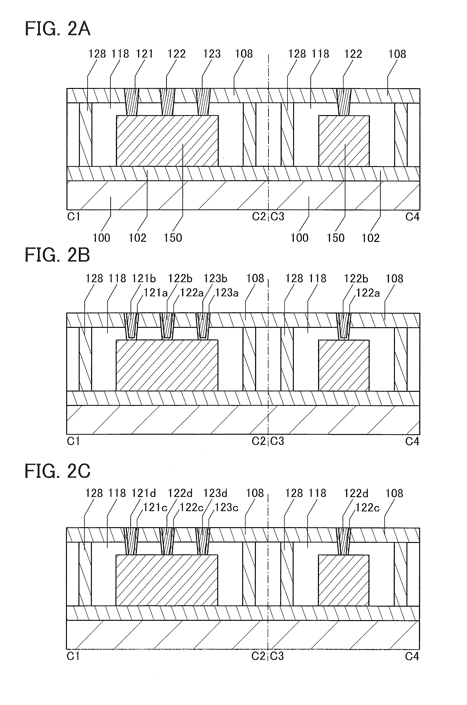
Provided is an element with stable electrical characteristics or a device including plural kinds of elements with stable electrical characteristics. The semiconductor device includes a first insulator, a transistor over the first insulator, a second insulator over the transistor, and a third insulator over the second insulator. The second insulator includes an opening reaching the first insulator. The opening is filled with a fourth insulator. The first insulator, the third insulator, and the fourth insulator each have a lower hydrogen-transmitting property than the second insulator.

Description

TECHNICAL FIELD[0001]The present invention relates to, for example, a transistor or a semiconductor device. The present invention relates to, for example, a method for manufacturing a transistor or a semiconductor device. The present invention relates to, for example, a display device, a light-emitting device, a lighting device, a power storage device, a memory device, a processor, or an electronic device. The present invention relates to a method for manufacturing a display device, a liquid crystal display device, a light-emitting device, a memory device, or an electronic device. The present invention relates to a driving method of a display device, a liquid crystal display device, a light-emitting device, a memory device, or an electronic device.[0002]Note that one embodiment of the present invention is not limited to the above technical field. The technical field of one embodiment of the invention disclosed in this specification and the like relates to an object, a method, or a m...

Claims


Application Information

Patent Timeline
Patent Type & Authority Applications(United States)
IPC IPC(8): H01L29/786
CPCH01L29/7869H01L29/78606H01L29/78603H01L29/78648H01L29/78696H01L27/1225H01L27/1248
Inventor YAMAZAKI, SHUNPEI
Owner SEMICON ENERGY LAB CO LTD
Why Eureka
Try Eureka