Semiconductor memory device

a memory device and memory technology, applied in the field of semiconductor memory devices including sense amplifiers, can solve the problem of shortened time for memory cells to reliably maintain data stored in cell capacitors, and achieve the effect of improving the data retention tim

Active Publication Date: 2016-06-09
SK HYNIX INC
View PDF1 Cites 4 Cited by
  • Summary
  • Abstract
  • Description
  • Claims
  • Application Information

AI Technical Summary

Benefits of technology

[0008]Various embodiments are directed to a semiconductor memory device having an improved data retention time for data of a memory cell.

Problems solved by technology

However, when current leakage increases, the length of time which memory cells may reliably maintain data that is stored in the cell capacitors is shortened.

Method used


Image

  • Semiconductor memory device
  • Semiconductor memory device
  • Semiconductor memory device

Examples


Embodiment Construction

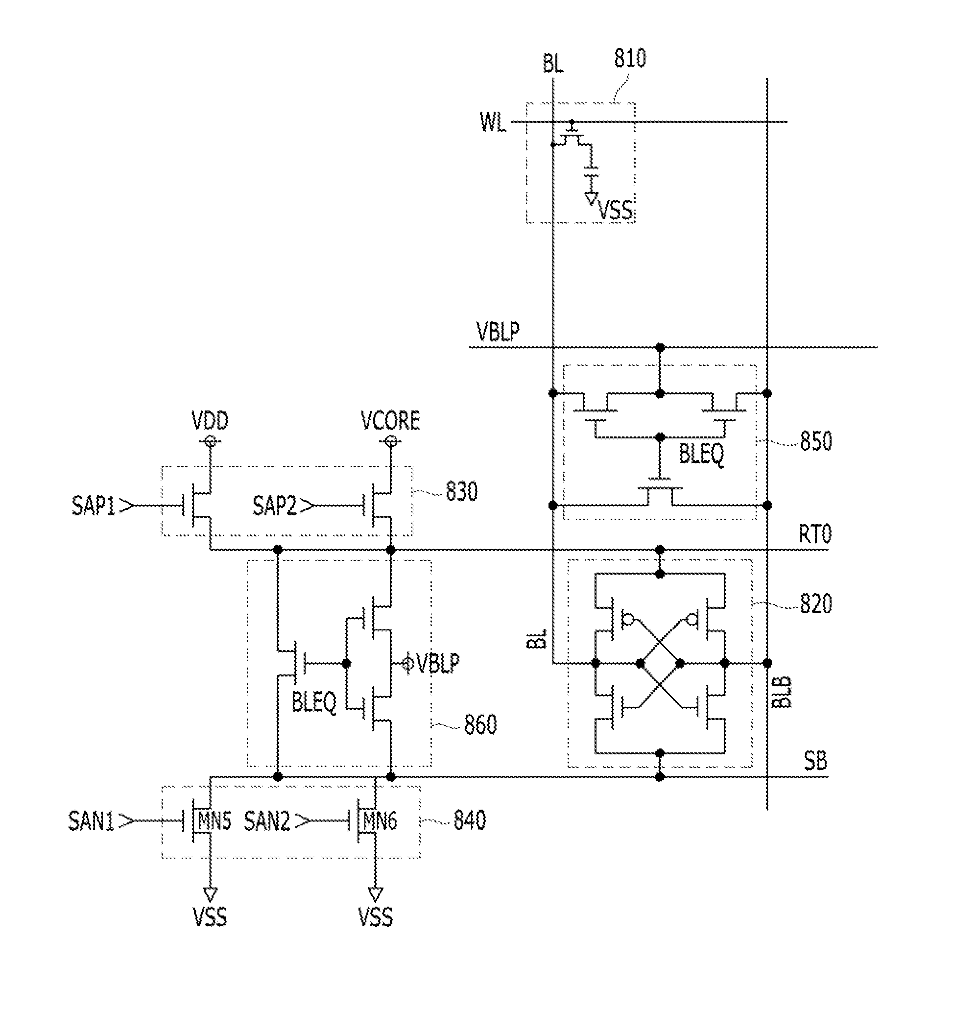
[0039]Various embodiments will be described below in more detail with reference to the accompanying drawings. The present invention may, however, be embodied in different forms and should not be construed as limited to the embodiments set forth herein. Rather, these embodiments are provided so that this disclosure will be thorough and complete, and will fully convey the scope of the present invention to those skilled in the art. Throughout the disclosure, like reference numerals refer to like parts throughout the various figures and embodiments of the present invention.

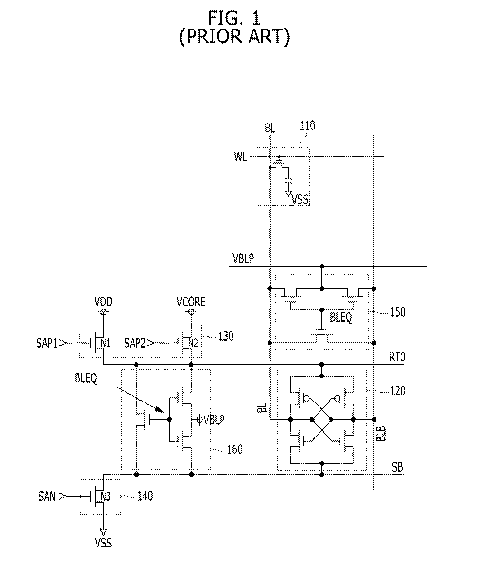
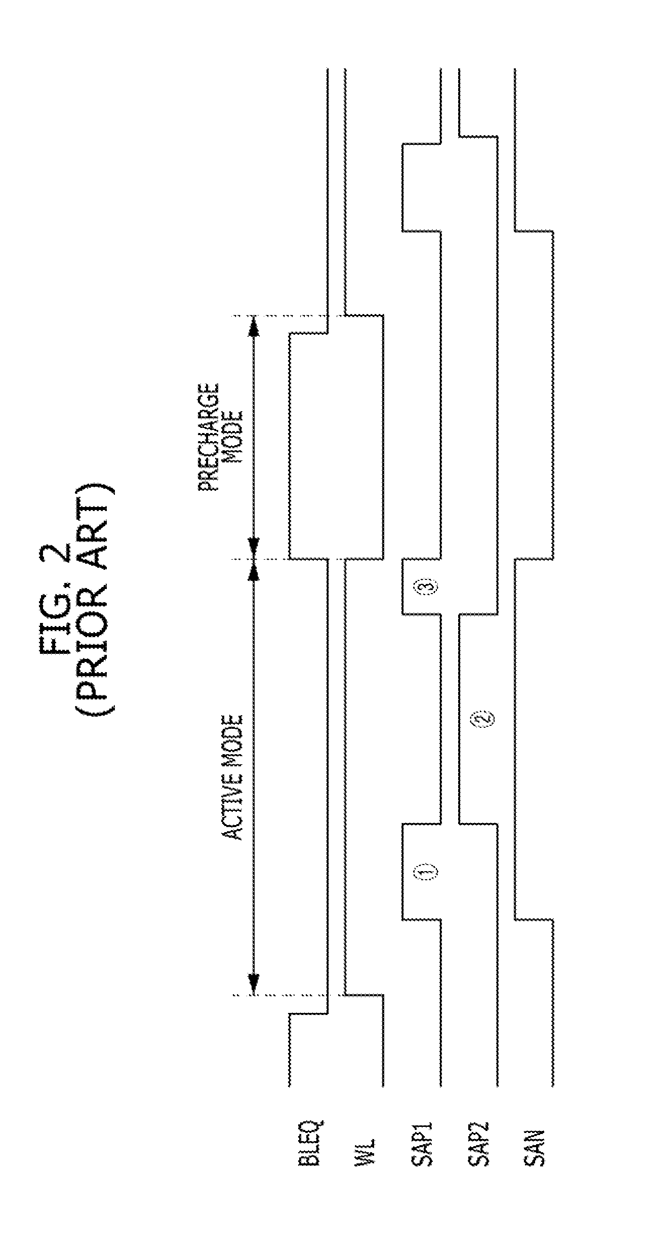
[0040]FIG. 1 is a circuit diagram illustrating a semiconductor memory device according to a comparative example of the present invention.

[0041]Referring to FIG. 1, the semiconductor memory device includes a bit-line pair BL and BLB including a positive bit-line BL and a negative bit-line BLB a memory cell 110, a sense amplifier 120, a pull-up driving unit 130, a pull-down driving unit 140, a first precharge unit 150, ...


PUM


Abstract

Disclosed is a semiconductor memory device including: a sense amplifier capable of sensing and amplifying data loaded on a data-line pair based on a pull-up driving voltage and a pull-down driving voltage; a pull-up driving unit capable of supplying a first voltage as the pull-up driving voltage for first and third active sections of an active mode, and supplying a second voltage having a voltage level lower than the first voltage as the pull-up driving voltage for a second active section of the active mode, between the first and third active sections of the active mode; and a pull-down driving unit capable of supplying a third voltage as the pull-down driving voltage for the first to third active sections of the active mode and for an initial section of a precharge mode after the active mode.

Description

CROSS-REFERENCE TO RELATED APPLICATIONS[0001]The present application claims priority of Korean Patent Application No. 10-2014-0174923 filed on Dec. 8, 2014, which is incorporated herein by reference in its entirety.BACKGROUND[0002]1. Field[0003]Exemplary embodiments of the present invention relate to a semiconductor design technology and, more particularly, to a semiconductor memory device including a sense amplifier.[0004]2. Description of the Related Art[0005]A Dynamic Random Access Memory (DRAM) device is a typical volatile semiconductor memory device. A DRAM memory cell has a cell transistor and a cell capacitor. The cell transistor serves to select the cell capacitor, and the cell capacitor serves to store electric charges that correspond to data.[0006]Since there is unintentional leakage of electric current in and out of the cell capacitors, the memory cell charges need to be periodically restored. This operation of restoring the charge in the cell capacitors is referred to as...

Claims


Application Information

Patent Timeline
Patent Type & Authority Applications(United States)
IPC IPC(8): G11C7/12G11C11/4074G11C11/4091G11C7/06
CPCG11C7/12G11C11/4091G11C11/4074G11C7/06G11C11/4094G11C5/145G11C5/147G11C7/065G11C11/4072
Inventor LEE, SUNG-YUBCHI, SUNG-SOO
Owner SK HYNIX INC
Why Eureka
Try Eureka