Device For Soldering Electrical Or Electronic Components

a technology for electrical or electronic components and devices, which is applied in the direction of metal working devices, manufacturing tools, and soldering apparatus, etc., can solve the problems of forming spatters, increasing the risk even further, and functional failure of components soldered in such a manner, so as to reduce the consumption of shielding gas

Active Publication Date: 2016-06-30
ERSA GMBH
View PDF9 Cites 4 Cited by
  • Summary
  • Abstract
  • Description
  • Claims
  • Application Information

AI Technical Summary

Benefits of technology

[0017]In order to minimize the consumption of shielding gas when employing the device in accordance with the invention under a shielding gas atmosphere, according to a further exemplary embodiment of the invention, at least one gas injec...

Problems solved by technology

If the solder, due to the forces of gravity, simply flows or falls back into the melting crucible now, there is the risk of spatters being formed when the solder hits the carrier fixing the soldering nozzles or the liquid level of the molten solder in the crucible, which spatters may lead to a functional failure of components having been soldered in such a manner if they get on the...

Method used


Image

  • Device For Soldering Electrical Or Electronic Components
  • Device For Soldering Electrical Or Electronic Components
  • Device For Soldering Electrical Or Electronic Components

Examples


Embodiment Construction

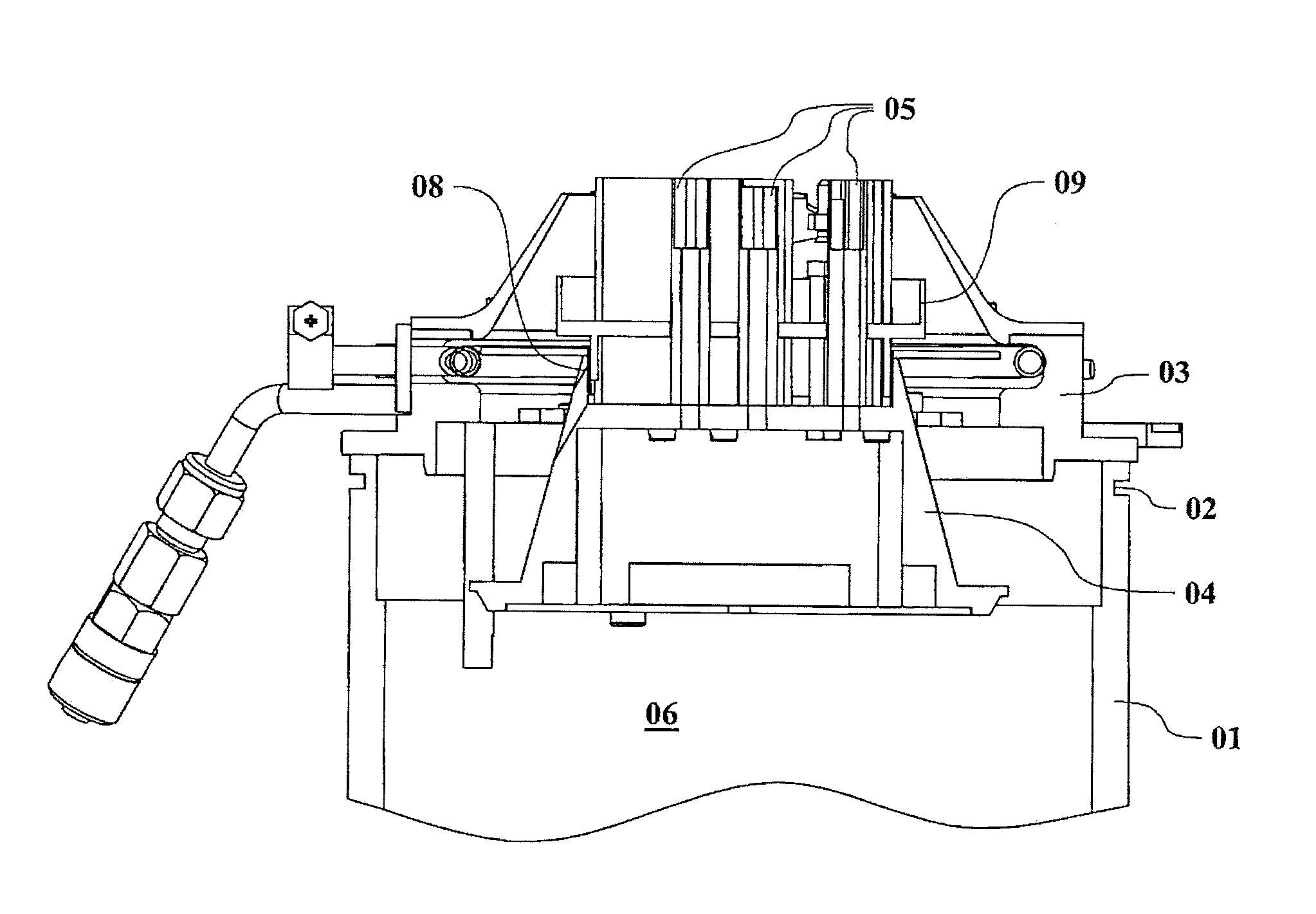
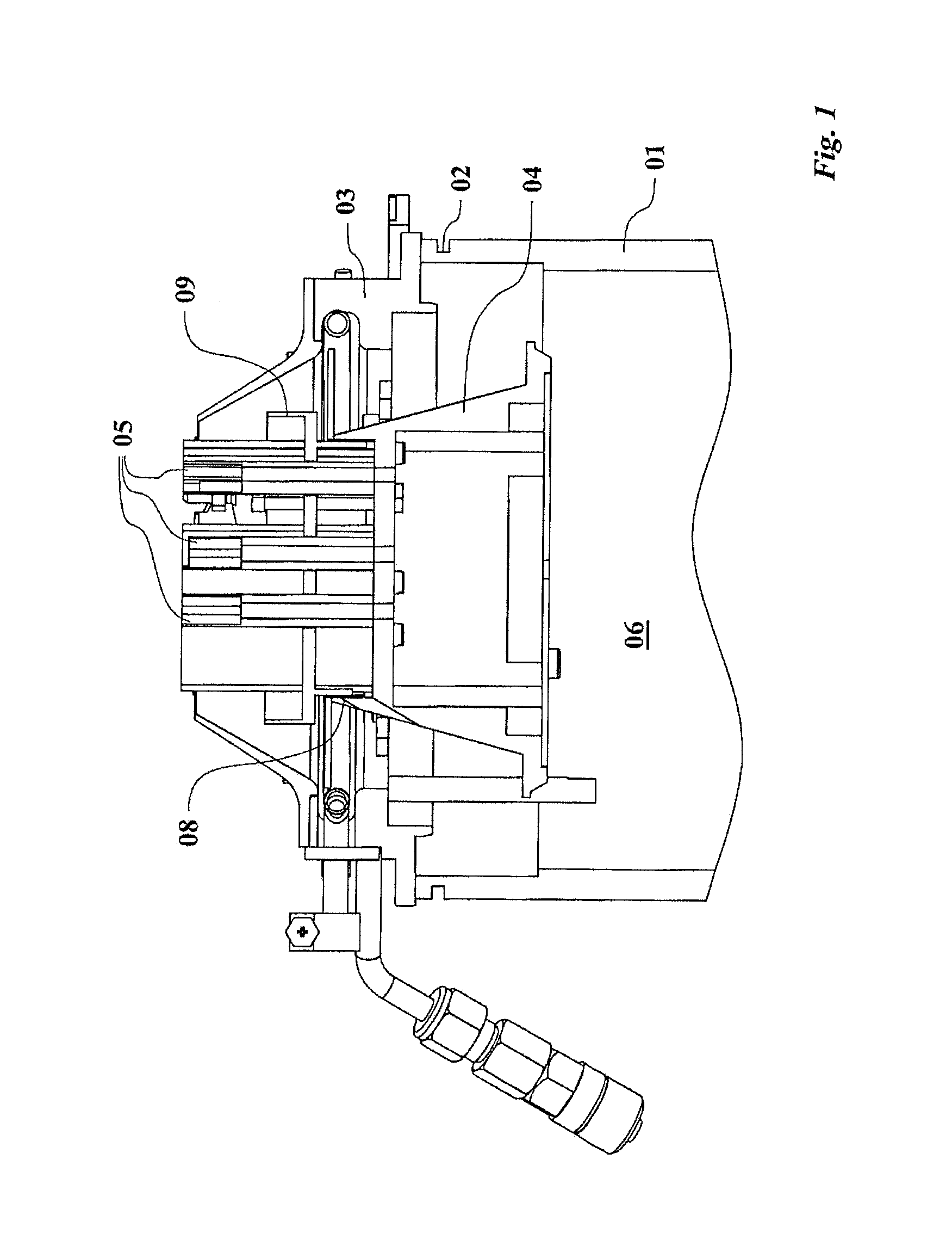
[0028]The device being illustrated in FIG. 1, for soldering electrical or electronic components, features a solder crucible 01, which is closed by a lid 03 at its upper collar 02. At the lid 03, a carrier 04 is arranged, on which a multitude of soldering nozzles 05 is arranged such that molten solder 06 that is situated in the solder crucible 01 can initially be conveyed out of the solder crucible 01 to the soldering nozzles 05 via a conveyor unit not being illustrated.

[0029]The stream of molten solder 06 leaves the soldering nozzles 05 at their upper ends, wets the soldering pins of the electrical or electronic components that are arranged on a printed circuit board and in this way produces a fixed and, in particular, electrically conductive soldering connection after it has solidified. Any excess solder, due to the forces of gravity, flows downwards, indirectly or directly back into the solder crucible 01.

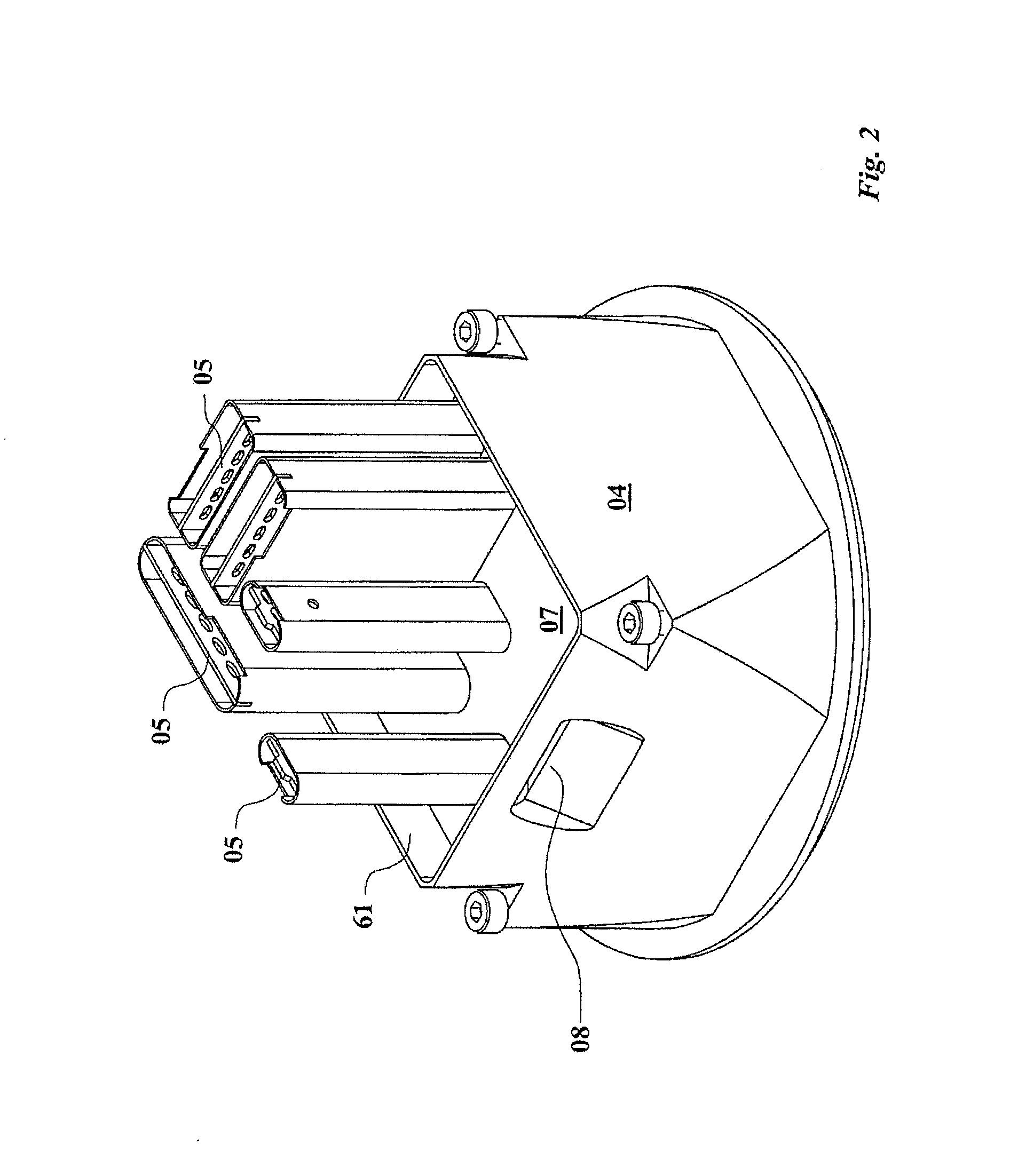
[0030]As it can in particular be taken from FIG. 2, the carrier 04, in this ...


PUM

PropertyMeasurementUnit
Distanceaaaaaaaaaa

Abstract

A device for soldering electrical or electronic components on a printed circuit board includes a soldering nozzle arrangement arranged above a solder crucible. The nozzle arrangement includes at least one carrier, on which at least one soldering nozzle is arranged. Molten solder is conveyed, using a conveyor unit, out of the solder crucible through the soldering nozzle to the components to be soldered. At least one discharge unit is arranged between a tip of the soldering nozzle and the carrier for any excess solder that has left the soldering nozzle. The discharge unit includes at least one baffle plate substantially surrounding the soldering nozzle.

Description

CROSS REFERENCE TO RELATED APPLICATION[0001]This application claims the priority benefit of German Patent Application No. 10 2014 119 682.1 filed on Dec. 29, 2014, which is fully incorporated herein by reference.STATEMENT REGARDING FEDERALLY SPONSORED RESEARCH OR DEVELOPMENT[0002]Not applicable.FIELD OF THE INVENTION[0003]The invention relates to a device for soldering electrical or electronic components on a printed circuit board.BACKGROUND OF THE INVENTION[0004]Devices of the type in question predominantly, but by no means exclusively, serve to solder electronic components on a printed circuit board, wherein the soldering pins of the components being arranged on the upper side of the printed circuit board or blank reach through the printed circuit board in recesses and project, at least slightly, beyond the lower side of the blank. Soldering is then either effected by advancing the blank to a point above a soldering nozzle unit that is fixedly arranged, with a solder wave leaving ...

Claims


Application Information

Patent Timeline
IPC IPC(8): B23K3/06H05K3/34B23K1/00
CPCB23K3/0607H05K2203/042H05K3/34B23K1/0016B23K2101/36B23K1/08B23K3/0653
Inventor VOLKER, STEFANSPACHMANN, EGON
Owner ERSA GMBH
Why Eureka
Try Eureka