Kinetically limited nano-scale diffusion bond structures and methods

a nano-scale diffusion bond, kinetic technology, applied in the direction of recording information storage, manufacturing tools, instruments, etc., can solve the problems of grain growth in polycrystalline materials, damage to the products they are forming, and damage to the components within the packag

Active Publication Date: 2016-06-30
CORNING INC +1
View PDF1 Cites 42 Cited by
  • Summary
  • Abstract
  • Description
  • Claims
  • Application Information

AI Technical Summary

Benefits of technology

[0007]In one embodiment bulk materials having a kinetically limited nano-scale diffusion bond is provided. The bulk materials having a kinetically limited nano-scale diffusion bond includes transparent material, absorbent opaque material and a diffusion bond. The transparent material has properties that allow an electromagnetic beam of a select wavelength to pass there through without more than minimal energy absorption. The absorbent opaque material has properties that significantly absorb energy from the electromagnetic beam. The diffusion bond is formed by the electromagnetic beam bonding the transparent material to the absorbent opaque material. Moreover, the diffusion bond has a thickness that is less than 1000 nm.
[0008]In yet another embodiment, bulk materials having a kinetically limited nano-scale diffusion bond is provided. In this embodiment, the bulk materials having a kinetically limited nano-scale diffusion bond include transparent material, absorbent material, an interfacial bond joint, undisturbed transparent material and undisturbed absorbent opaque material. The transparent material has properties that allow an electromagnetic beam of a select wavelength to pass there through without more than minimal energy absorption. The absorbent material has properties that significantly absorb energy from the electromagnetic beam. The bond is formed by the electromagnetic beam bonding the transparent material to the absorbent material. The bond interfacial bond joint is less than 1000 nm in thickness. The undisturbed transparent material and undisturbed absorbent material are located outside the less than 1000 nm bond. Moreover, the undisturbed transparent material and undisturbed absorbent material are not affected by the formation of the bond.
[0009]In still another embodiment, a method of forming a kinetically limited nano-scale diffusion bond in bulk materials is provided. The method includes positioning a first surface to be bonded of a transparent material against a second surface to be bonded of an absorbent opaque material. The transparent material has properties that allow an electromagnetic beam of a select wavelength to pass there through without more than minimal energy absorption and the absorbent opaque material has properties that significantly absorb energy from the electromagnetic beam. Pressure on the transparent material and absorbent opaque material is then applied so that the first surface to be bonded of the transparent material is in contact with the second surface to be bonded of the absorbent opaque material. An electromagnetic beam is then selectively passed through the transparent material to the second surface to be bonded of the absorbent opaque material. The electromagnetic beam then creates a kinetically limited nano-scale diffusion bond between the transparent material and the absorbent opaque material.

Problems solved by technology

The temperatures used can be in the order of 600-1000° C. These high temperatures can result in harm to the products they are forming.
For example, when forming packages for devices, high temperatures used to form the bonds in the package risk damaging components that are within the package.
This also results in grain growth in polycrystalline materials and alters their physical properties.
Moreover, undesirable compounds form in bond regions with the use of high temperatures over long formation times that can affect the strength or toughness of the bond.
Additionally, differences in the thermal expansion coefficients of the materials bonded using diffusion bonding techniques can lead to the generation of interfacial stresses as the assembly cools from high temperatures.
These stresses often result in crack generation.
The size of the cracks that are created due to interfacial stresses tends to scale with the size of the interaction zone of the materials being joined.
Since typical diffusion bonding creates realtively large interaction zones, the cracks that are generated also tend to extend several microns to millimeters.
Brittle materials will spontaneously fail catastrophically even under small loads if the cracks exceed the critical flaw size.
So larger cracks will likely result in reduced reliability and service life.
For this reason, traditional diffusion bonding techniques have had limited success in creating mechanically robust bonds between materials with dissimilar thermal expansion coefficients.
However, this approach has several disadvantages.
The flux used for soldering is prone to cause contamination which is difficult to detect especially if the bond is used to seal the enclosure.
The strength of the bond is inferior to that of the bulk materials, and these solder alloys are susceptible to corrosion if exposed to harsh environments.
However, it is difficult with these techniques to determine the integrity of the bond and the bond strength is far inferior to the strength of the bulk materials.
Other methods using adhesives are used to form bonds however, the bonds are inherently weaker and non-hermetic.

Method used


Image

  • Kinetically limited nano-scale diffusion bond structures and methods
  • Kinetically limited nano-scale diffusion bond structures and methods
  • Kinetically limited nano-scale diffusion bond structures and methods

Examples


Embodiment Construction

[0028]In the following detailed description, reference is made to the accompanying drawings, which form a part hereof, and in which is shown by way of illustration specific embodiments in which the inventions may be practiced. These embodiments are described in sufficient detail to enable those skilled in the art to practice the invention, and it is to be understood that other embodiments may be utilized and that changes may be made without departing from the spirit and scope of the present invention. The following detailed description is, therefore, not to be taken in a limiting sense, and the scope of the present invention is defined only by the claims and equivalents thereof.

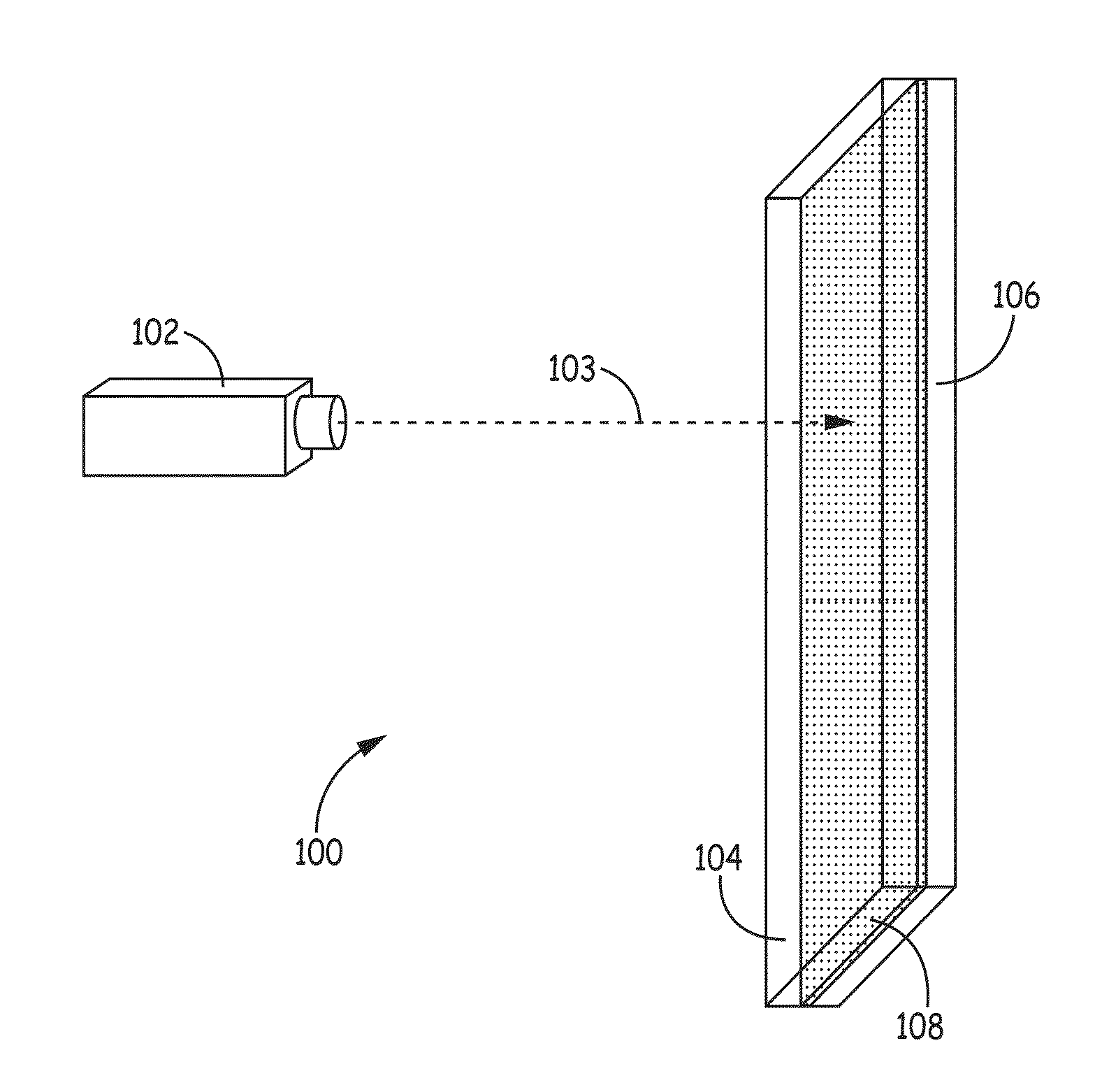
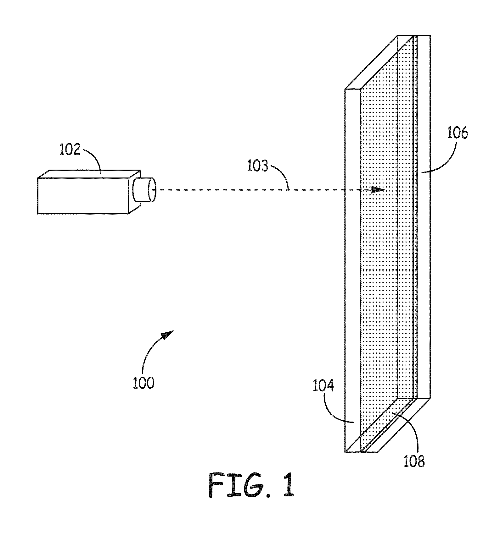
[0029]Embodiments of the present invention provide for the bonding of dissimilar bulk materials with a rapid room-temperature process. The bulk materials being bonded include a transparent material 104 (non-metal ((insulator)) material) and an absorbent opaque material 106 (metal ((conductor)) material) as ge...


PUM

PropertyMeasurementUnit
thicknessaaaaaaaaaa
thickaaaaaaaaaa
thickaaaaaaaaaa

Abstract

Bulk materials having a kinetically limited nano-scale diffusion bond is provided. The bulk materials having a kinetically limited nano-scale diffusion bond includes transparent material, absorbent opaque material and a diffusion bond. The transparent material has properties that allow an electromagnetic beam of a select wavelength to pass there through without more than minimal energy absorption. The absorbent opaque material has properties that significantly absorb energy from the electromagnetic beam. The diffusion bond is formed by the electromagnetic beam bonding the transparent material to the absorbent opaque material. Moreover, the diffusion bond has a thickness that is less than 1000 nm.

Description

[0001]This Application claims priority to U.S. Provisional Application Ser. No. 62 / 096,706, same title herewith, filed on Dec. 24, 2014, which is incorporated in its entirety herein by reference.BACKGROUND[0002]Bonding different types of bulk material together to form a bonded article has many applications in a variety of industries. For example, in the semiconductor industry the ability to bond an insulator material to a conductive material is highly desired. Moreover, being able to attach an insulative material, such as sapphire, to a metal, like titanium, has many applications including the formation of packaging for photonic and medical devices. Another example industry that desires the ability to effectively attach sapphire to titanium is the manufacturing of high end jewelry. This method also has applicability for bonding sapphire windows in high vacuum systems, and military and space vehicles.[0003]Traditional methods of bonding these types of material together use high tempe...

Claims


Application Information

Patent Timeline
Patent Type & Authority Applications(United States)
IPC IPC(8): B32B7/04B32B9/04B32B37/14B23K26/32B23K26/20B23K20/22B32B15/04B23K20/02
CPCB32B7/04B32B15/04B32B9/041B23K20/023B23K26/32B23K2203/54B23K20/22B32B37/14B23K2203/18B23K2203/14B23K26/20B23K20/02B23K2103/52B23K2103/172B23K2103/14B23K2103/54B23K2103/18B32B17/061B32B2311/18B32B2310/0887B82Y30/00B32B2307/412
Inventor SANDLIN, MICHAEL S.RUBEN, DAVID A.KARAM, RAYMOND M.ROUSSOS, GEORGESWYNNE, THOMAS M.
Owner CORNING INC
Why Eureka
Try Eureka