Advanced process flow for high quality fcvd films

Active Publication Date: 2016-07-07
APPLIED MATERIALS INC
View PDF3 Cites 19 Cited by
  • Summary
  • Abstract
  • Description
  • Claims
  • Application Information

AI Technical Summary

Benefits of technology

[0008]In one embodiment, a method of forming a flowable CVD film is provided. The method includes forming a dielectric film on a substrate by reacting a silicon containing precursor, a nitrogen containing precursor, and an oxygen containing precursor in a processing chamber at a temperature of about 100 degrees Celsius or less at a pressure between about 0.5 Torr and about 10 Torr. The method sequentially includes treating the dielectric film by exposing the dielectric film to one or more ion species in an ion implantation process and subsequently exposing the dielectric film to oxygen radicals to cure the dielectric film. The cured dielectric film may be annealed by exposing the dielectric film to water vapor at a temperature less than about 500 degrees Celsius.
[0009]In another embodiment, a method of forming a flowable CVD film is provided. The method includes forming a dielectric film on a substrate by reacting a silicon containing precursor, a nitrogen containing precursor, and an oxygen containing precursor in a processing chamber at a temperature of about 100 degrees Celsius or less at a pressure between about 0.5 Torr and about 1

Problems solved by technology

As device geometries shrink and thermal budgets are reduced, void-free filling of high aspect ratio spaces becomes increasingly difficult due to limitations of existing deposition processes.
However, FCVD films generally exhibit low density as deposited when compared to thermally deposited oxides.
Such temperatures are often beyond the thermal budgets of device mate

Method used


Image

  • Advanced process flow for high quality fcvd films
  • Advanced process flow for high quality fcvd films
  • Advanced process flow for high quality fcvd films

Examples


Embodiment Construction

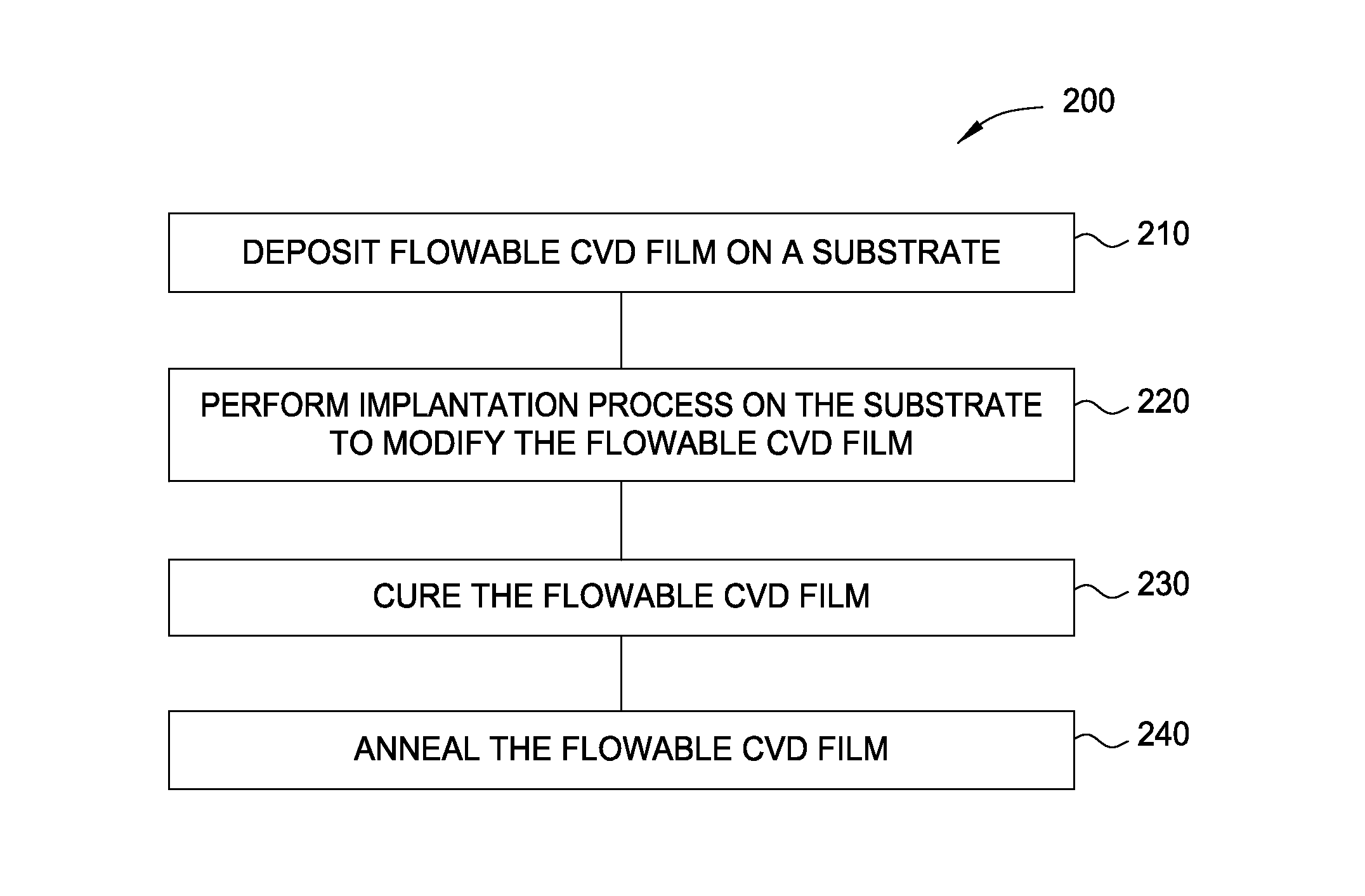
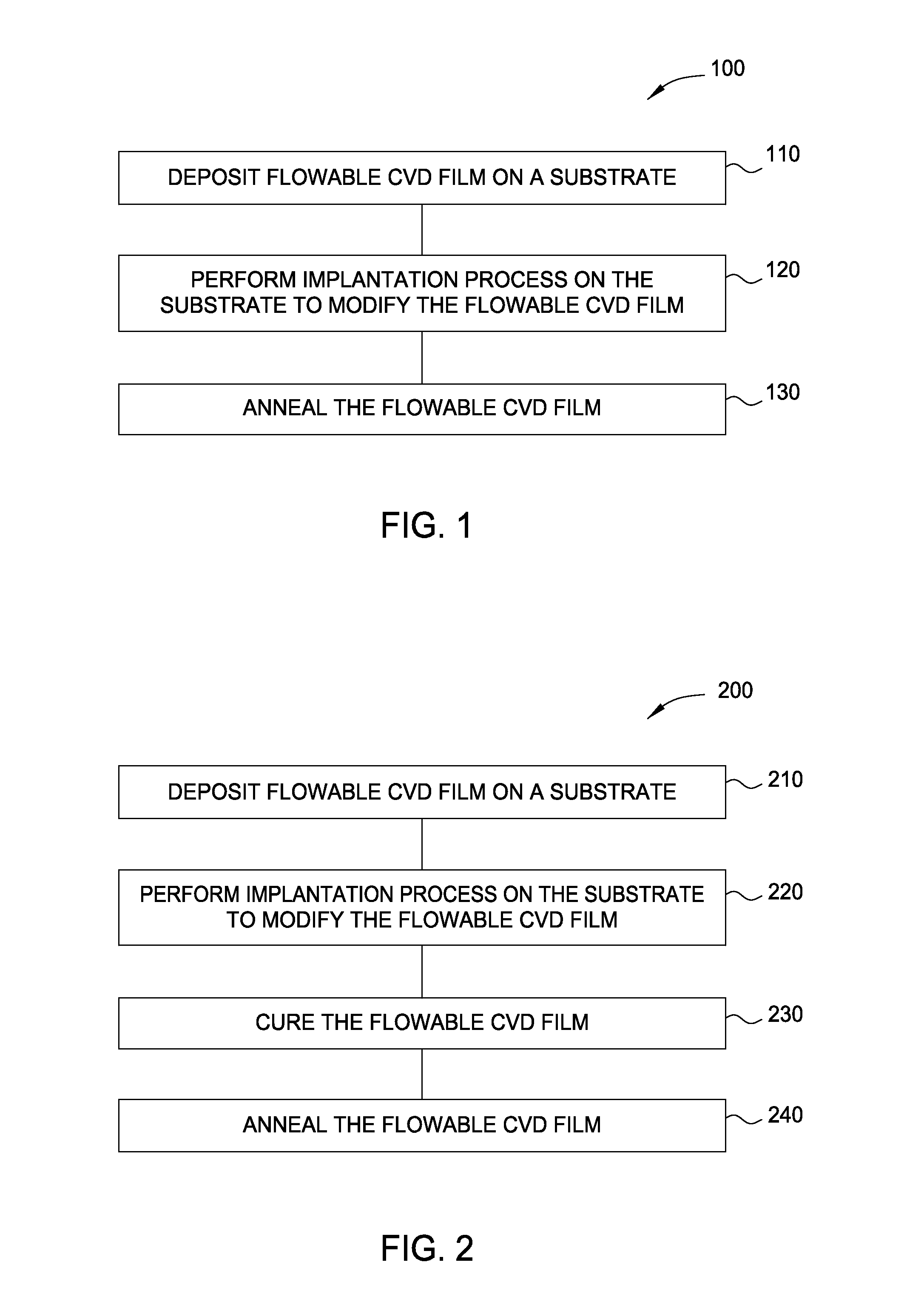
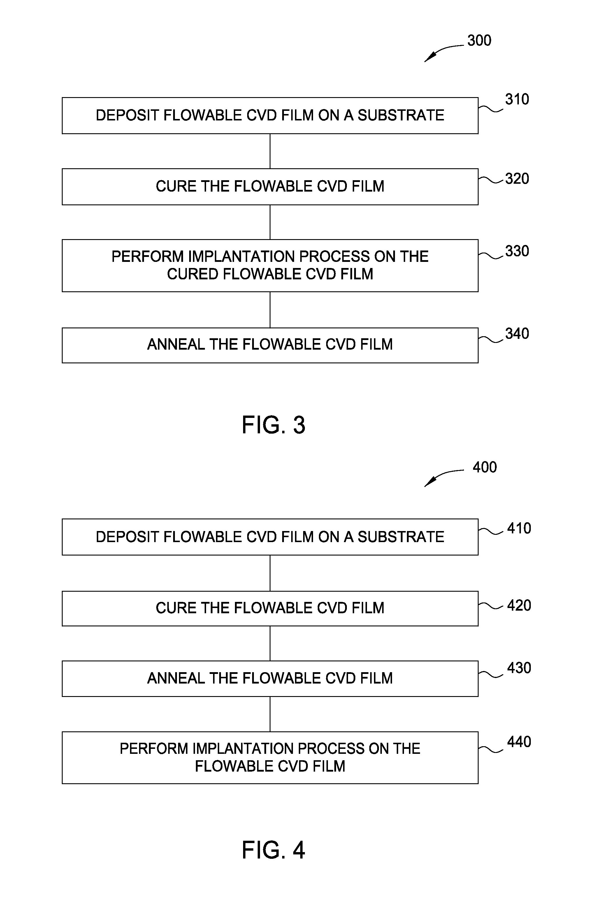
[0021]Embodiments described herein relate to methods for forming flowable chemical vapor deposition (FCVD) films suitable for high aspect ratio gap fill applications, among other applications. Various process flows described include ion implantation processes utilized to treat a deposited FCVD film to improve dielectric film density and material composition. Ion implantation processes, curing processes, and annealing processes may be utilized in various sequence combinations to form dielectric films having improved densities at temperatures without exceeding the thermal budget of device materials. Improved film quality characteristics include reduced film stress and reduced film shrinkage when compared to conventional FCVD film formation processes.

[0022]FIG. 1 illustrates operations of a method 100 for forming an FCVD film. At operation 110, an FCVD film is deposited on a substrate. The substrate generally has HAR features formed thereon and one or more processing chambers may be ut...


PUM

PropertyMeasurementUnit
Temperatureaaaaaaaaaa

Abstract

Embodiments described herein relate to methods for forming flowable chemical vapor deposition (FCVD) films suitable for high aspect ratio gap fill applications. Various process flows described include ion implantation processes utilized to treat a deposited FCVD film to improve dielectric film density and material composition. Ion implantation processes, curing processes, and annealing processes may be utilized in various sequence combinations to form dielectric films having improved densities at temperatures within the thermal budget of device materials. Improved film quality characteristics include reduced film stress and reduced film shrinkage when compared to conventional FCVD film formation processes.

Description

CROSS-REFERENCE TO RELATED APPLICATIONS[0001]This application claims benefit of U.S. provisional patent application No. 62 / 100,888, filed Jan. 7, 2015, the entirety of which is hereby incorporated by reference.BACKGROUND[0002]1. Field[0003]Embodiments of the present disclosure generally relate to a methods of forming dielectric materials on a substrate. More specifically, embodiments provided herein relate to process flow for forming high quality flowable chemical vapor deposition (FCVD) films.[0004]2. Description of the Related Art[0005]In semiconductor processing, devices are being manufactured with continually decreasing feature dimensions. Often, features utilized to manufacture devices at these advanced technology nodes include high aspect ratio structures and it is often necessary to fill gaps between the high aspect ratio structures with an insulating material. Examples where insulating materials are utilized for gap fill applications include shallow trench isolation, inter-m...

Claims


Application Information

Patent Timeline
IPC IPC(8): C23C16/56C23C16/32C23C14/48C23C16/36C23C16/40C23C16/30C23C16/34
CPCC23C16/56C23C16/308C23C16/325C23C16/345C23C14/48C23C16/401C23C16/402C23C16/30C23C16/36C23C16/045
Inventor NEMANI, SRINIVAS D.CHEN, ERICAGODET, LUDOVICXUE, JUNYIEH, ELLIE Y.
Owner APPLIED MATERIALS INC
Why Eureka
Try Eureka