
Display device

a technology of display device and display screen, which is applied in the direction of solid-state devices, optics, instruments, etc., can solve the problems of low light use efficiency, achieve the effects of improving light use efficiency, simple configuration, and low power consumption

Inactive Publication Date: 2016-07-21
JAPAN DISPLAY INC
View PDF4 Cites 24 Cited by
  • Summary
  • Abstract
  • Description
  • Claims
  • Application Information

AI Technical Summary

Benefits of technology

The patent is trying to solve the problem of complicated and expensive displays made using fluorescent dyes. The invention aims to improve the use efficiency of light from a light source and achieve low power consumption with a simple configuration, even without the use of a color filter. The display device includes a fluorescent material layer, a reflective layer that absorbs and emits phosphor, and a barrier with an inclined plane. This simple configuration allows for efficient use of light and reduced power consumption.

Problems solved by technology

More specifically, color filters used for color display cut many wavelength components from light emitted from a white light source, and have a low use efficiency of light.

Method used


Image

  • Display device
  • Display device
  • Display device

Examples


first embodiment

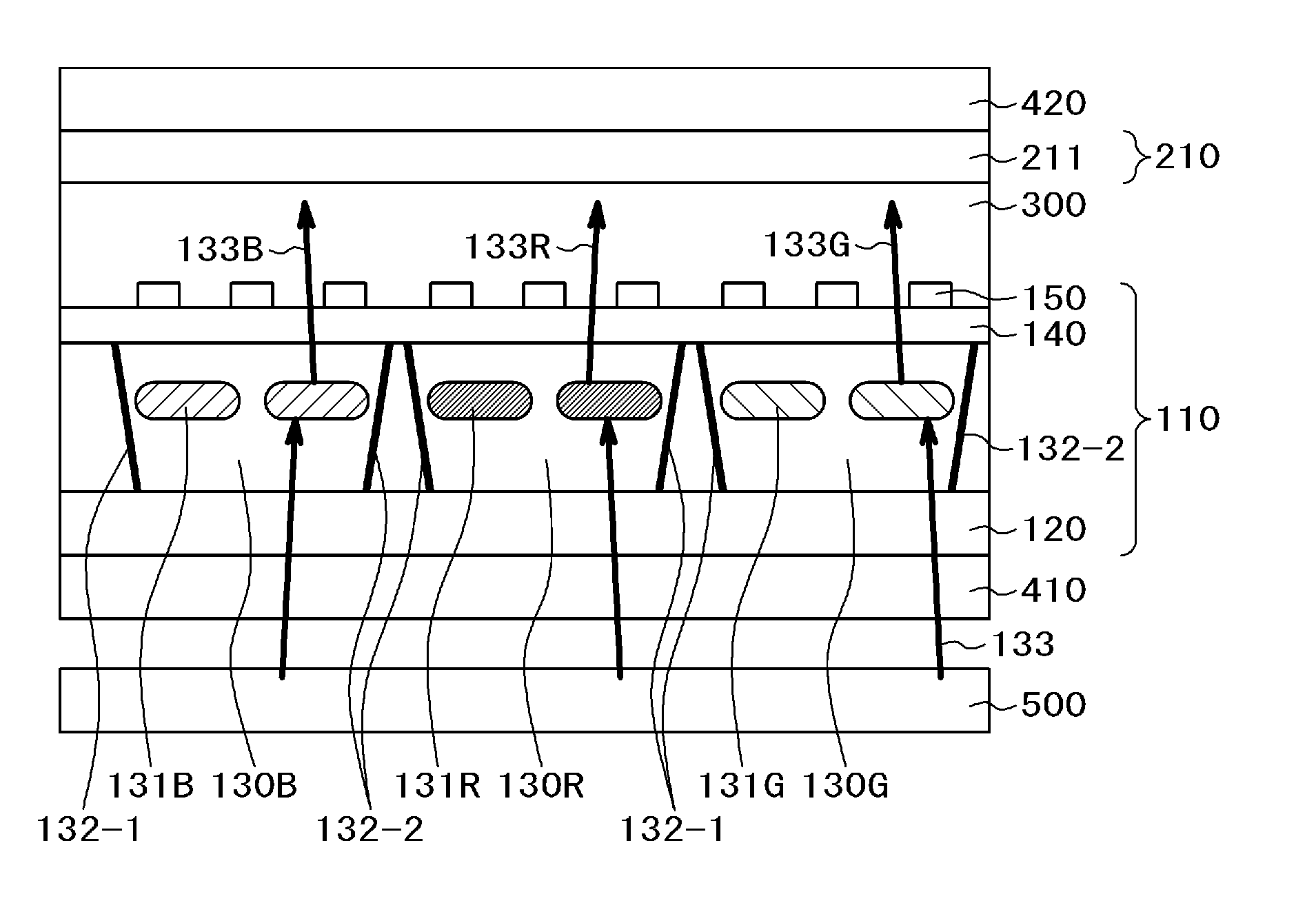
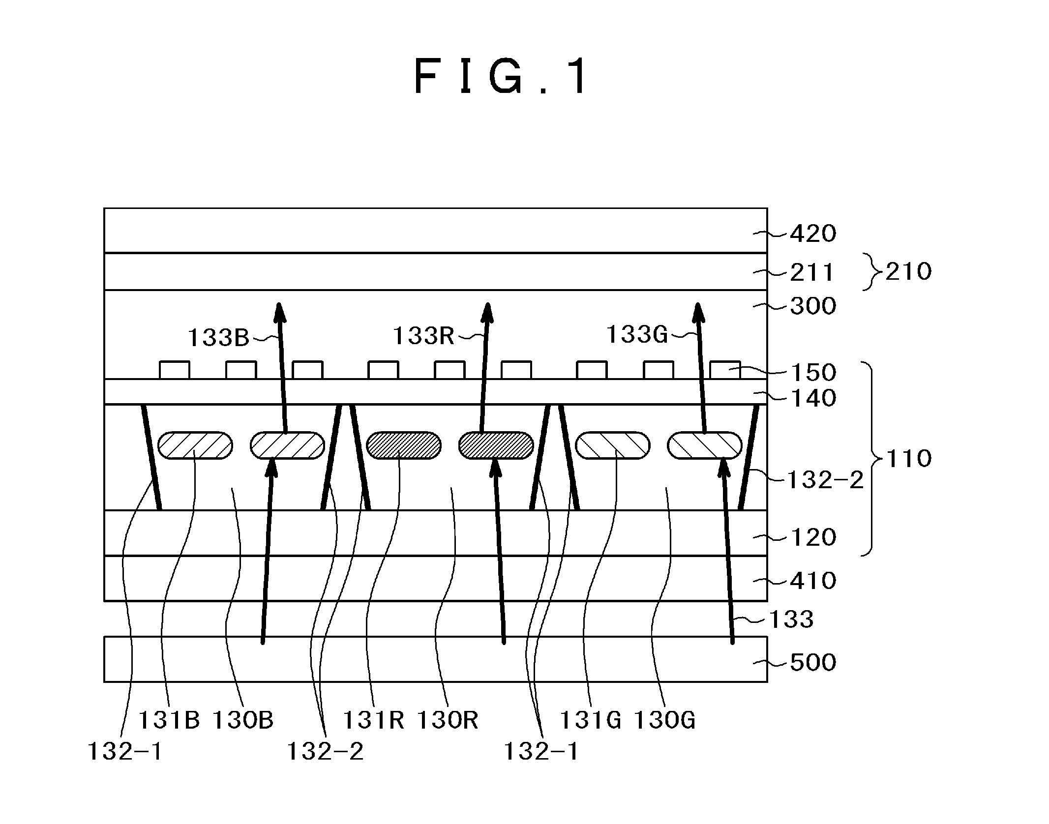
[0020]A liquid crystal display device according to a first embodiment of the present invention will be described with reference to FIGS. 1 to 6.

[0021]FIG. 6 is a schematic plan view of a liquid crystal display device according to the first embodiment. As illustrated in FIG. 6, a liquid crystal display device 100 includes a TFT substrate (an array substrate) 110, a counter substrate 210, and a liquid crystal layer (not illustrated) between the TFT substrate 110 and the counter substrate 210. The TFT substrate 110 is attached to the counter substrate 210 with a sealing material 104. On a display region 105 of the TFT substrate 110, scanning signal lines, picture signal lines, pixels disposed on a matrix configuration, a wavelength conversion layer including quantum rods and disposed at a location corresponding to the transmission region of the pixel, and other components are formed. The pixel includes a thin film transistor (TFT), a pixel electrode, a common electrode, and other compo...

second embodiment

[0042]A second embodiment of the present invention will be described with reference to FIG. 7. Matters described in the first embodiment but not described in the second embodiment are also applicable to the second embodiment unless otherwise specified.

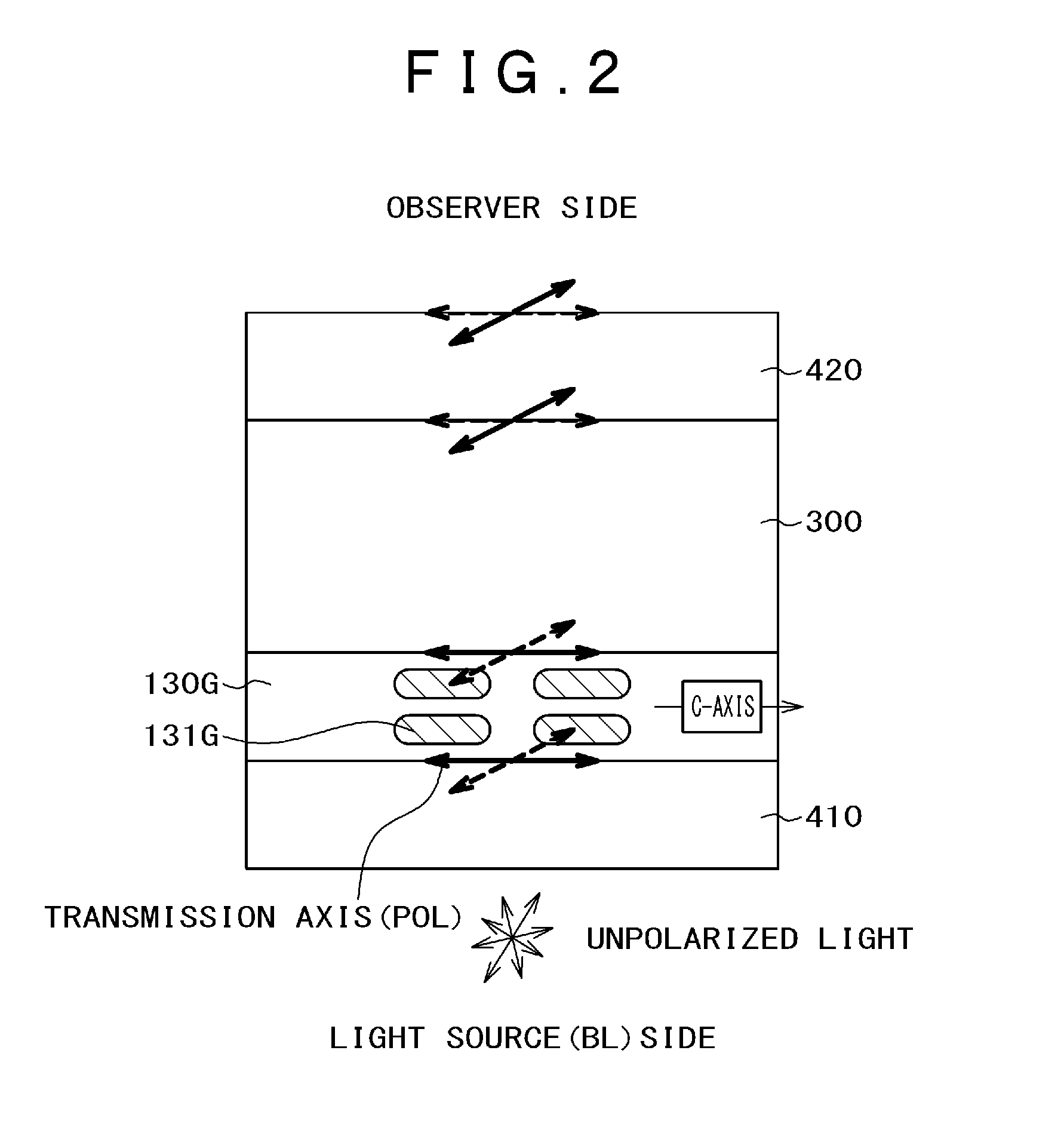
[0043]FIG. 7 is a schematic diagram for explaining the polarization states of light in a liquid crystal display device according to the embodiment (in the case in which the transmission axes of the first and second polarizers 410 and 420 are in parallel with the C-axis of the quantum rod). In FIG. 7, only the first and second polarizers 410 and 420, the wavelength conversion layer 130G including the green quantum rod 131G, and the liquid crystal layer 300 are illustrated, and other components are omitted.

[0044]In FIG. 7, the second polarizer 420, the liquid crystal layer 300, the first polarizer 410, and the wavelength conversion layer 130G including the green quantum rod 131G are disposed from an observer in this order. To the first p...


PUM


Abstract

There is provided a display device that can improve the use efficiency of light from a light source and achieve low power consumption with a simple configuration even in the case in which no color filter is used. A display device includes a substrate having a display region and a TFT disposed on the display region, wavelength conversion layers each including a columnar quantum rod and disposed on a region corresponding to the display region, and a light source that excites the quantum rods.

Description

CLAIM OF PRIORITY[0001]The present application claims priority from Japanese patent application JP 2015-9657 filed on Jan. 21, 2015, the content of which is hereby incorporated by reference into this application.BACKGROUND OF THE INVENTION[0002](1) Field of the Invention[0003]The present invention relates to a display device.[0004](2) Description of the Related Art[0005]A liquid crystal display device, which is one of display devices, has merits, such as high display quality, thin thickness, light weight, and low power consumption. The applications of the liquid crystal display device are expanding because of these merits. The liquid crystal display device is used in various applications including a portable monitor, such as a mobile telephone monitor and a digital still camera monitor, a desktop personal computer monitor, monitors for printing and design, a medical monitor, and a liquid crystal television.[0006]More specifically, mobile electronic devices, which are represented by ...

Claims


Application Information

Patent Timeline
IPC IPC(8): G02F1/1335G02F1/1368
CPCG02F1/133617G02F1/1368G02F1/133512G02F2001/133614Y10S977/765Y10S977/952B82Y20/00G02F1/133528B82Y30/00G02F1/136222
Inventor MIKI, HIROHISAARAKI, SHIGESUMINISHIYAMA, KAZUHIRO
Owner JAPAN DISPLAY INC
Learn More