

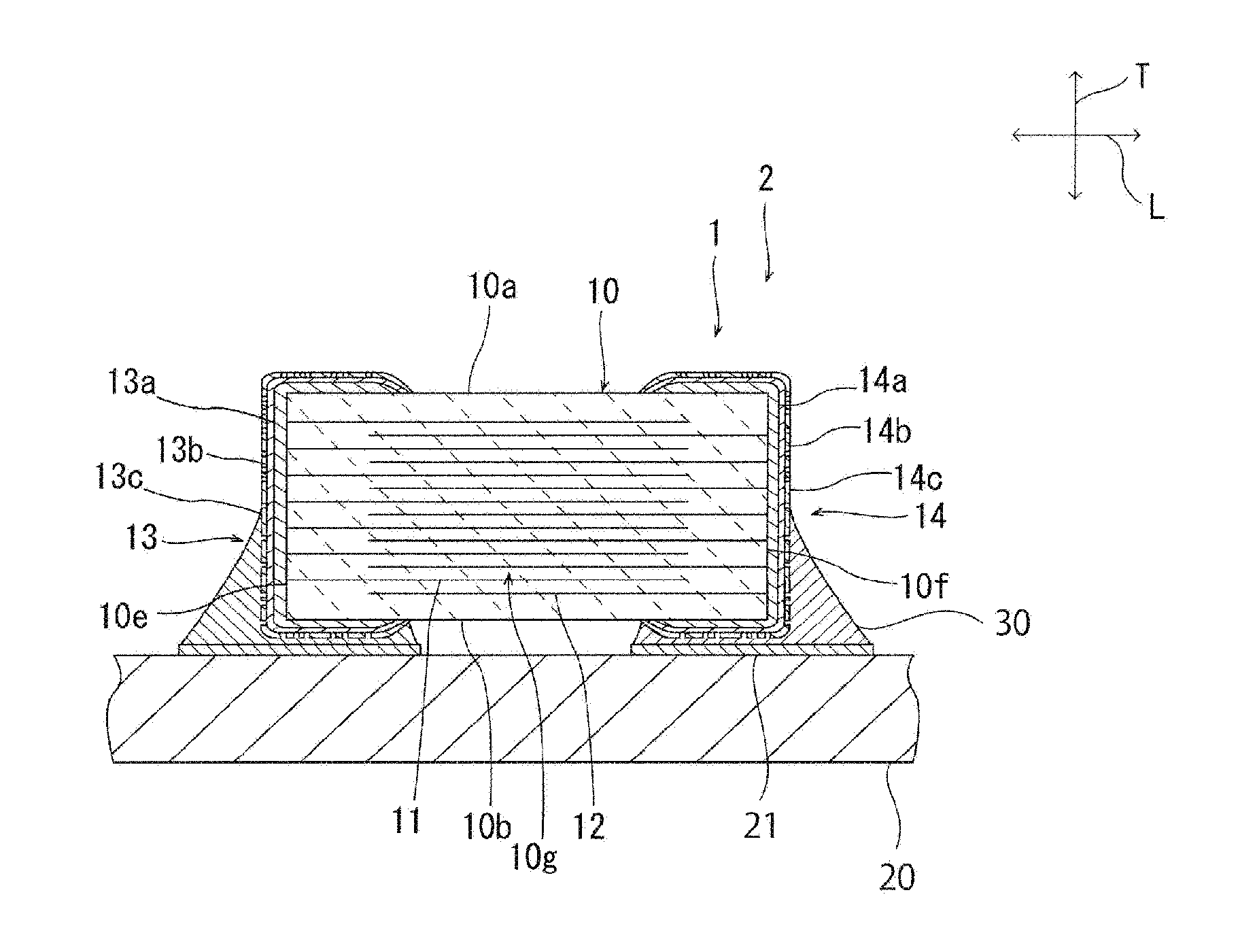
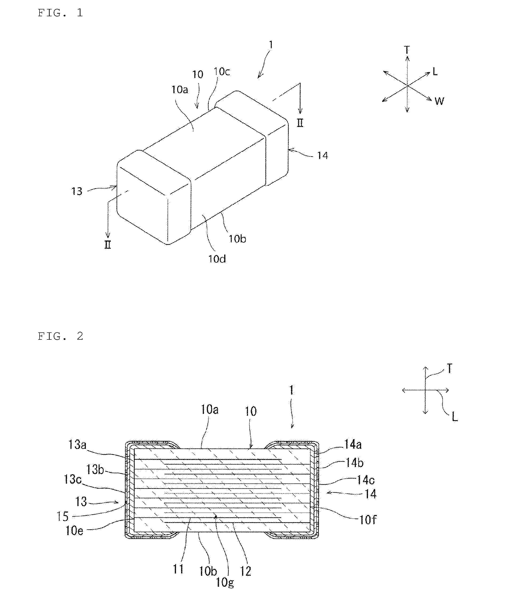
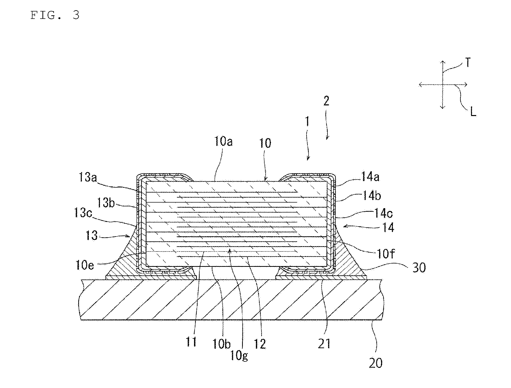
Electronic component and electronic component-mounted structure
a technology of electronic components and components, applied in the direction of printed circuit non-printed electric components association, sustainable manufacturing/processing, final product manufacturing, etc., can solve the problems of ceramic element cracking, solder itself cracking, etc., and achieve the effect of improving the reactivity with the conductive resin adhesive 30
- Summary
- Abstract
- Description
- Claims
- Application Information
AI Technical Summary
Benefits of technology
Problems solved by technology
Method used
Image

Examples
example 1
[0067]An electronic component (multilayer ceramic capacitor) having the following structure was produced according to the method described in the above preferred embodiments. The formed Pd plating layer had the film thickness of 0.02 μm.
[0068]Conditions in forming Ni plating layer[0069]Barrel: Diameter 67 mmφ-Width 110 mm[0070]Media material: Solder shot 0.7 mmφ[0071]Media amount: 60 mL[0072]Chip: Longitudinal dimension: 1.0 mm, Width dimension: 0.5 mm,[0073]Thickness dimension: 0.5 mm[0074]Number of revolutions of barrel: 60 rpm[0075]Plating solution: Composition
[0076]Nickel sulfate 365 g / L
[0077]Nickel chloride 65 g / L
[0078]Boric acid 40 g / L[0079]Temperature: 60° C.[0080]pH: 4.2[0081]Current: 8 A[0082]Time: 167 minutes (aimed at 5 μm)
[0083]Conditions in forming Pd plating layer[0084]Barrel: Diameter 67 mmφ-Width 110 mm[0085]Media material: Solder shot 0.7 mmφ[0086]Media amount: 60 mL[0087]Chip: Longitudinal dimension: 1.0 mm, Width direction: 0.5 mm,[0088]Thickness direction: 0.5 mm...
PUM
| Property | Measurement | Unit |
|---|---|---|
| thickness | aaaaa | aaaaa |
| width | aaaaa | aaaaa |
| length | aaaaa | aaaaa |
Abstract
Description
Claims
Application Information