Display device

a technology of a display device and a display case, which is applied in the direction of display/control unit casings, electrical apparatus casings/cabinets/drawers, circuit electrostatic discharge protection, etc., can solve the problems of poor contact, peeling off, and reduced protection against emi or esd, so as to reduce the ground impedance improve the durability of the conductive element, and avoid poor contact.

Inactive Publication Date: 2016-07-21
INNOLUX CORP
View PDF4 Cites 0 Cited by
  • Summary
  • Abstract
  • Description
  • Claims
  • Application Information

AI Technical Summary

Benefits of technology

[0008]An objective of the invention is to provide a display device which can improve the adhesion of the conductive element.
[0019]As mentioned above, in the display device according to the invention, the quantities of the conductive portions which are spaced apart each other and located at the ground zone of the circuit board respectively along the first direction and the second direction are plural, and the conductive element is disposed on the conductive pattern and electrically connected to the conductive portions. Thus, compared with conventional technology, it can reduce the ground impedance of the conductive element and the ground zone and improve the durability of the conductive element against the stress due to the lateral force. Therefore, it can avoid poor contact, separation, or other problems of the conductive element so as to improve the protection of the display device from EMI and ESD.

Problems solved by technology

Moreover, because of more powerful functions, faster operating speed, and increasingly dense and complex electronic circuits of modern electronic products, the problem of electromagnetic interference (EMI) or electrostatic discharge (ESD) becomes a major challenge of circuit design.
However, the conductive element on the circuit board by adhesion not only increases working-hours for adhesion but also results in poor contact, peeling off, or other problems of the conductive element, so the protection against EMI or ESD is reduced.

Method used


Image

  • Display device
  • Display device
  • Display device

Examples


Embodiment Construction

[0027]The present invention will be apparent from the following detailed description, which proceeds with reference to the accompanying drawings, wherein the same references relate to the same elements.

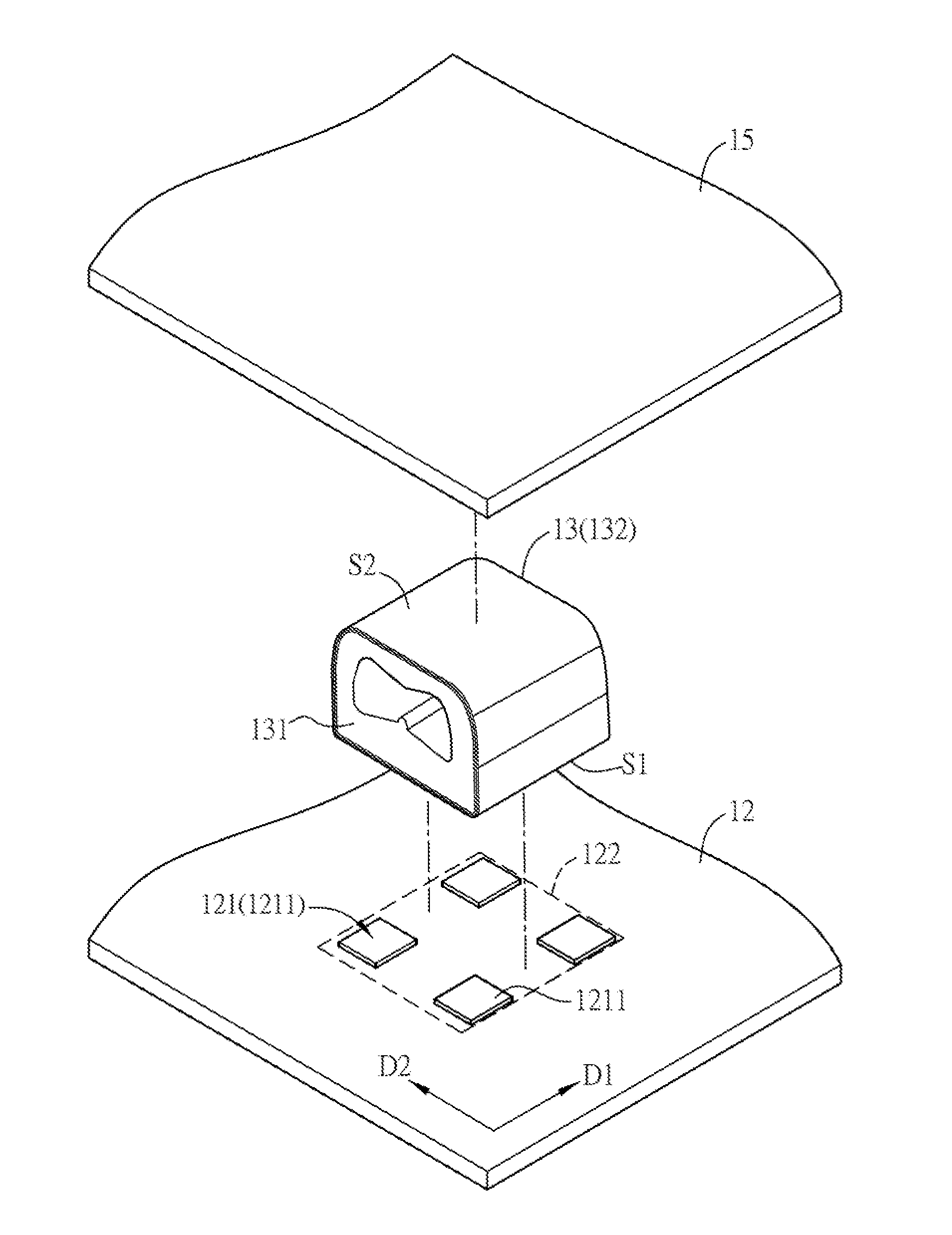
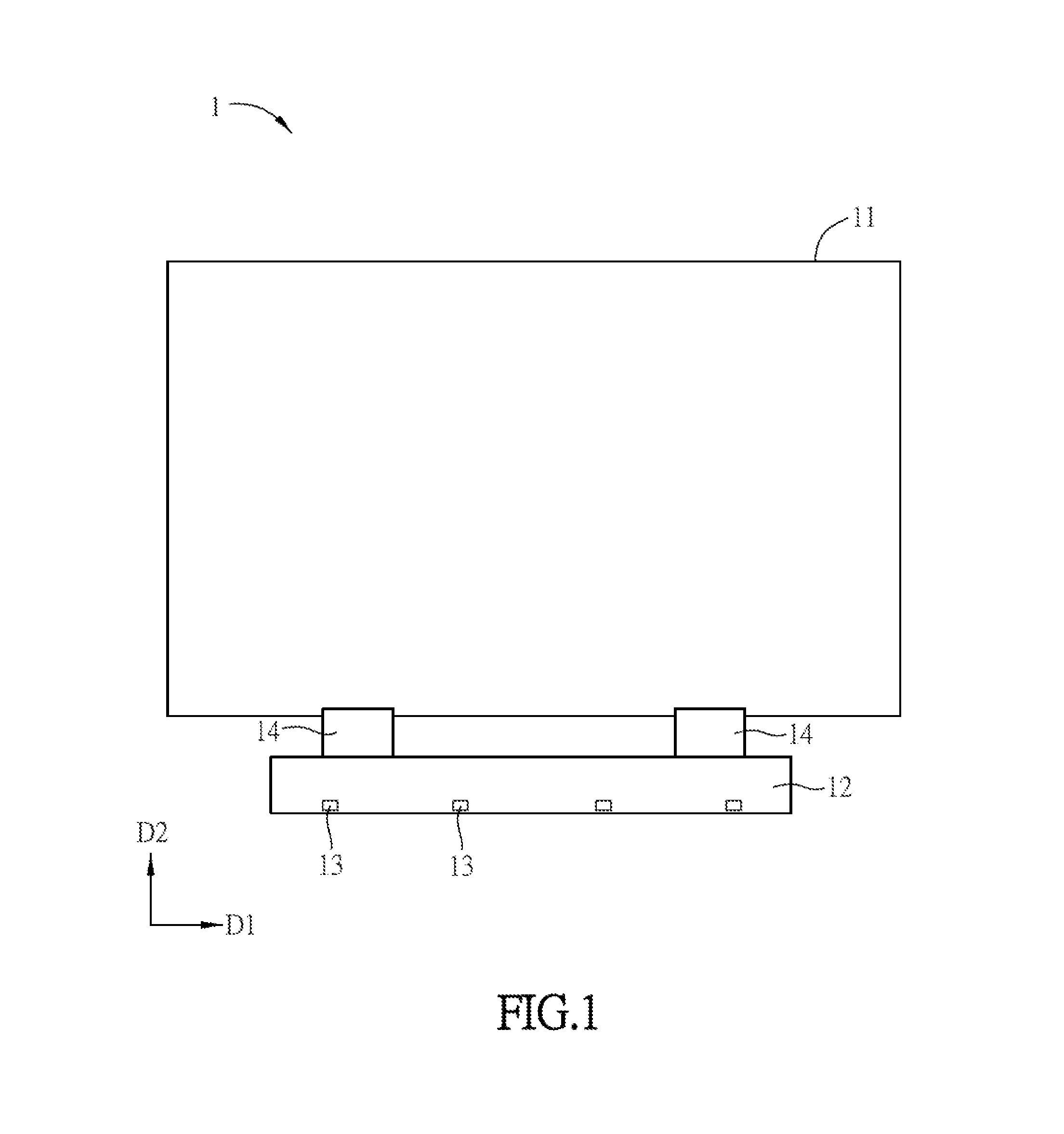
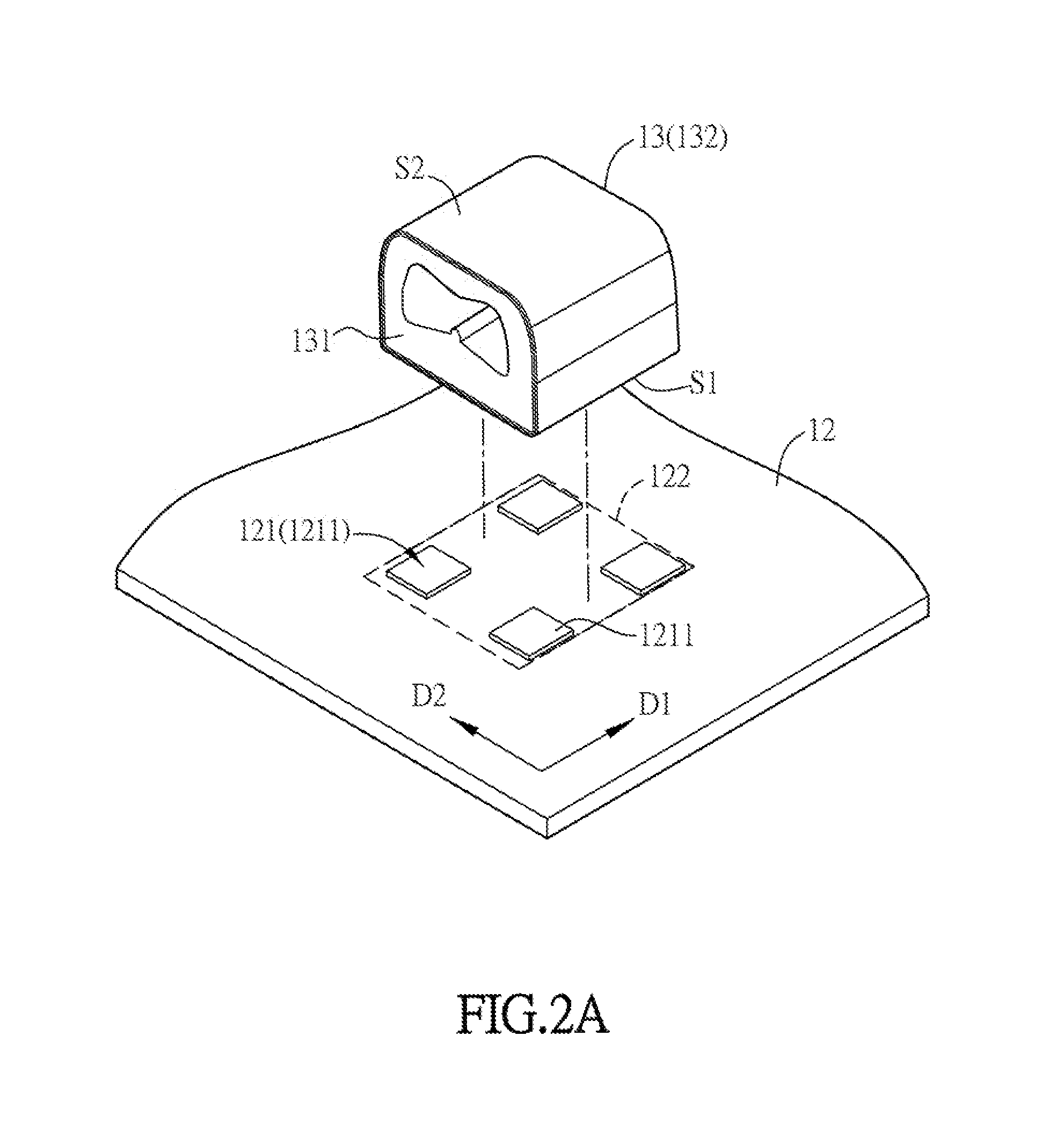
[0028]Referring to FIGS. 1 to 2C, FIG. 1 is a schematic diagram of a display device 1 according to an embodiment of the invention, FIG. 2A is a schematic diagram of the connection between the circuit board 12 and the conductive element 13 of the display device 1 in FIG. 1, FIG. 2B is a top view of the conductive pattern 121 on the circuit board 12 in FIG. 2A, and FIG. 2C is a schematic diagram of the connection of the circuit board 12, the conductive element 13, and the metal element 15 in the display device 1.

[0029]The display device 1 may be a liquid crystal display device or an organic light emitting diode display device, for example but not limited to, a display screen, a tablet computer, a smart phone, a global positioning system device, a laptop, or an electronic device having a...


PUM


Abstract

A display device includes a display panel, a circuit board, and a conductive element. The circuit board is adjacent to the display panel and electrically connected to the display panel. The circuit board has at least a conductive pattern configured at a ground zone, and the conductive pattern has a plurality of conductive portions spaced apart each other. The quantities of the conductive portions respectively arranged along a first direction and a second direction are plural, and the first direction is substantially perpendicular to the second direction. The conductive element is disposed on the conductive pattern, and the conductive element is electrically connected to the conductive portions.

Description

CROSS REFERENCE TO RELATED APPLICATIONS[0001]This Non-provisional application claims priority under 35 U.S.C. §119(a) on Patent Application No(s). 104101821 filed in Taiwan, Republic of China on Jan. 20, 2015, the entire contents of which are hereby incorporated by reference.BACKGROUND OF THE INVENTION[0002]1. Field of Invention[0003]The invention relates to a display device and, in particular, to a display device with a PCB.[0004]2. Related Art[0005]With the advance of technology, flat display devices have been broadly applied to various fields and especially to liquid crystal display devices or organic light emitting diode display devices. Because flat display devices have superior characteristics of thin and light body, low power consumption, and no radiation, they gradually replace conventional cathode ray tube display devices and are applied to various electronic products, such as mobile phones, portable media devices, laptops, televisions, and so on.[0006]Moreover, because of ...

Claims


Application Information

Patent Timeline
Patent Type & Authority Applications(United States)
IPC IPC(8): H05K9/00H05K5/00H05K1/02H05K5/04
CPCH05K9/0054H05K5/04H05K5/0026H05K2201/10128H05K1/0216H05K9/0067H05K1/0259H05K5/0017H05K1/0215H05K1/0271H05K2201/0133H05K2201/0314H05K2201/10257
Inventor TSAI, WEI-JENLEE, HUI-LANGYANG, YING-WEN
Owner INNOLUX CORP
Why Eureka
Try Eureka