Microfluidic channels for thermal management of microelectronics

a microfluidic channel and microelectronic technology, applied in the direction of semiconductor devices, semiconductor/solid-state device details, electrical apparatus, etc., can solve the problems of disrupting the already-established semiconductor fabrication process, and achieve better in-plane tolerances, finer or more complex features, and mechanical or chemical properties. good

Inactive Publication Date: 2016-07-28
NUVOTRONICS
View PDF7 Cites 7 Cited by
  • Summary
  • Abstract
  • Description
  • Claims
  • Application Information

AI Technical Summary

Benefits of technology

[0017]As a thermal spreader of the present invention may be created from the combination of multiple parts, sealing these parts may be important when fluids in liquid or gas state are involved. Thus, in another of its aspects the present invention may provide a copper gasket that is microfabricated as a good way of making one or more of these seals. Other materials than copper may be used that are softer or that have particular mechanical or chemical properties that are desirable. For example, an indium gasket may be created and then coated with a gold layer to make it more chemically inert or impart other desirable mechanical properties. Additionally, the gasket does not necessarily have to be electrically conductive. While such gaskets may be formed in a mold, it is possible that stamping or cutting by other means may be preferred. By using microfabrication techniques such as electroplating the gasket in a patterned mold, such as a photoresist mold, and then removing the gasket from the mold or dissolving the mold material, or by chemical etching, the gasket may have an unusual pattern, which may be necessary given the small features required to attach to microelectronics. The gasket may, for example, be patterned to join flange regions on two metal surfaces while not obstructing flow between integrated nozzles, plumbing, or areas for return flow. The microfabricated gasket can have better in-plane tolerances and finer or more complex features than gaskets formed by traditional operations such as progressive stamping. Additionally, the thickness of the microfabricated gasket may be varied over the surface of the gasket in well controlled steps. This could be used to provide different areas of the seal with different pressures, make up extra tolerances, or provide for different crush of the gasket in different areas.
[0018]The attachment of a microfabricated thermal spreader of the present invention to a microelectronic device to be cooled is also an important consideration. If the thermal spreader is a copper-based material or other standard metal, it is important to important to consider methods to match the coefficient of thermal expansion between the microelectronics device (consider it a semiconductor integrated circuit in bare die form) and the thermal spreader. Matching the coefficient of thermal expansion could be achieved using an engineered pattern in the copper to limit the thermal expansion mismatch or provide flexible compliance where the two materials are joined. The material used to join the integrated circuit to the thermal spreader may be a solder, a conductive epoxy, an anisotropic adhesive, or the thermal spreader may be grown on the backside of the IC—either the entire wafer of ICs at once, a group of them, or on a chip-by-chip basis. Alternatively, a stack of materials of varying thickness values and coefficients of thermal expansion may be employed to reduce the stress from IC to the predominate material of the thermal spreader. Such a stack could be electroplated as part of the fabrication process for the thermal spreader.
[0019]In addition to the fluidic connections, mechanical connections may also be required, which can be fabricated by defining alignment features which take advantage of the realizable geometric tolerance of the microfabrication process. These alignment features may use the outer dimensions or inner dimensions of the fluidic channels to which they are attached.

Problems solved by technology

In either case, these are new process steps that disrupt the already-established semiconductor fabrication processes in practice (and may require re-design of the circuits, as well).

Method used


Image

  • Microfluidic channels for thermal management of microelectronics
  • Microfluidic channels for thermal management of microelectronics
  • Microfluidic channels for thermal management of microelectronics

Examples


Embodiment Construction

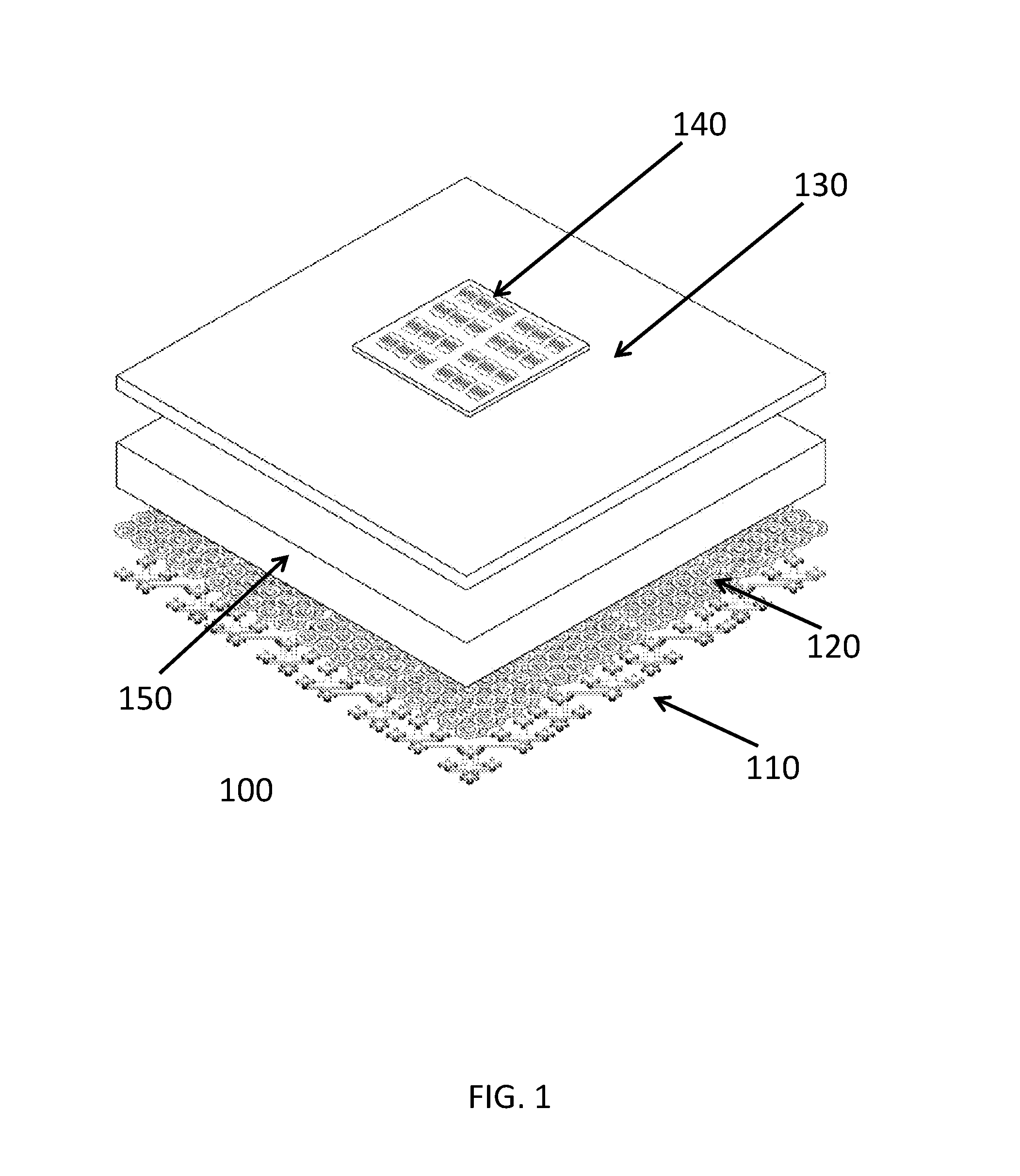
[0033]Referring now to the figures, wherein like elements are numbered alike throughout, FIG. 1 shows an exploded view illustrating several concepts of the present invention. A microelectronic device 140 (here assumed to be a GaN HEMT array) is bonded with a stress transition stack (or other thermal interface material) 130 to an integrated thermal spreader 150. Within the integrated thermal spreader 150 are micro-structured thermal spreaders 120 to which fluid is distributed and optionally retrieved using a fluidic manifold 110 here shown as a fluidic distribution network.

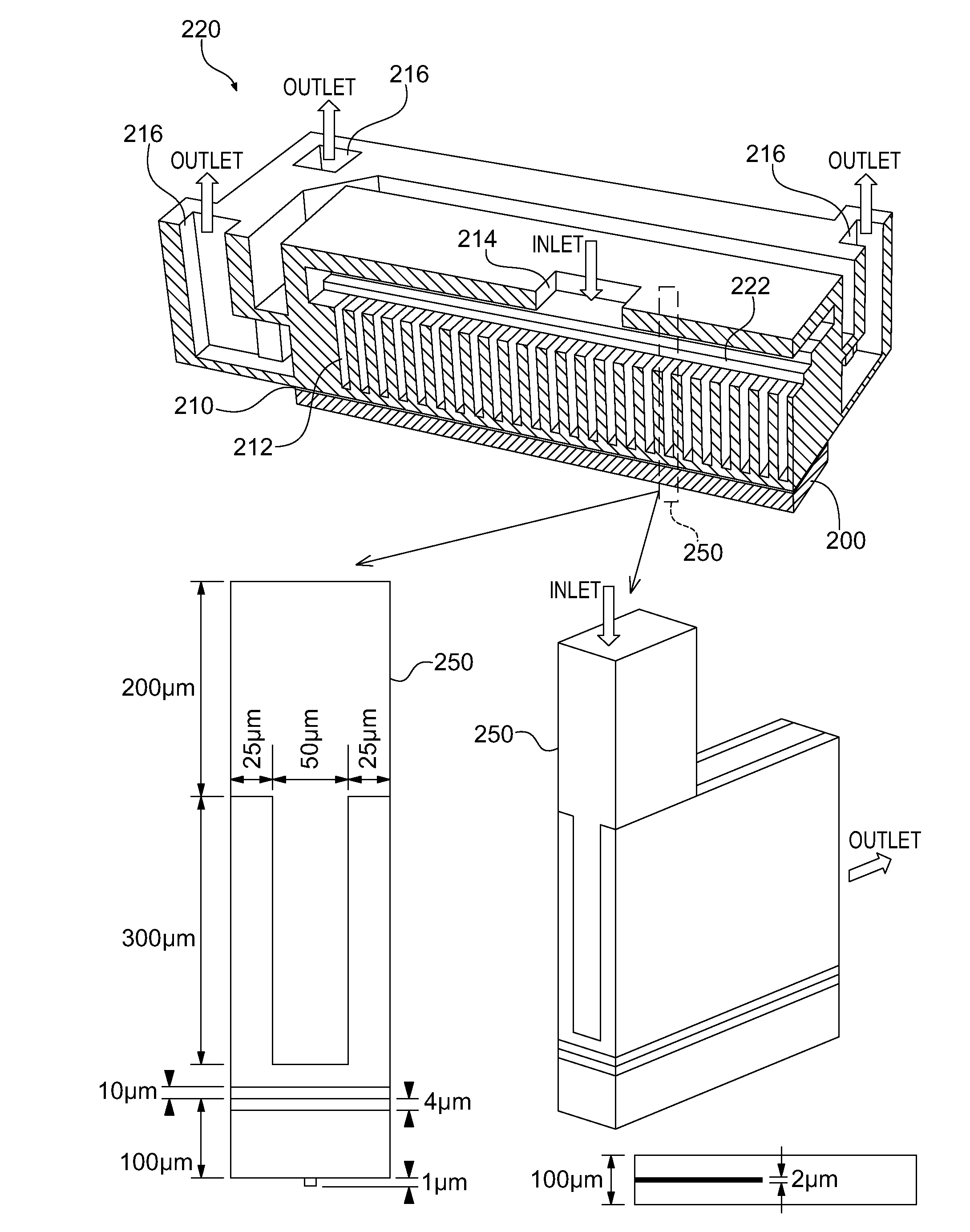
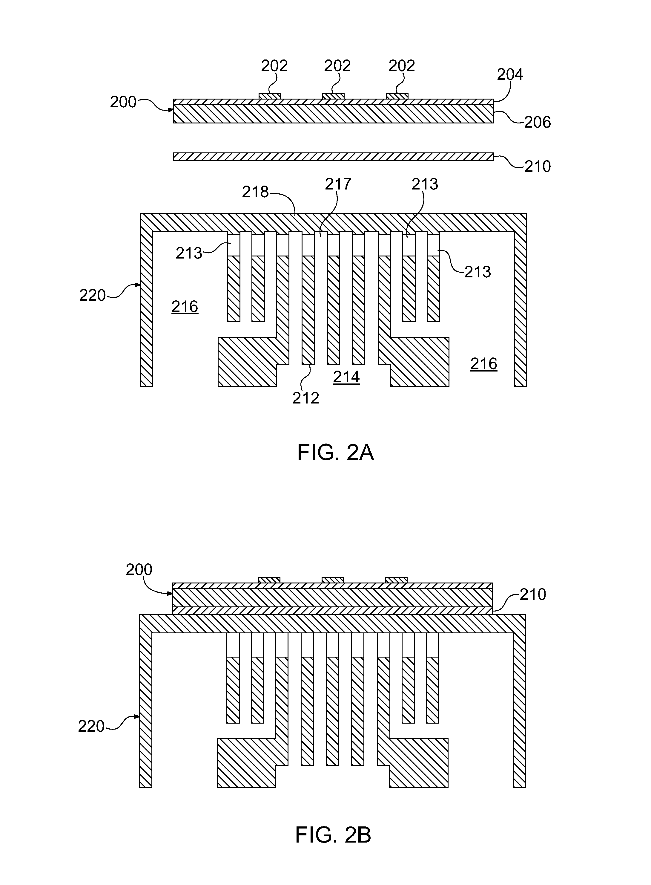
[0034]FIG. 2A illustrates an exploded view in cross section of FIG. 2B, which may be viewed as including three constitutive parts: i) a microelectronics device 200, which may be an integrated circuit such as a GaN HEMT RF amplifier; ii) a microfabricated thermal spreader 220 with integrated fluidic heat exchanger and flow regions; and iii) a stress transition stack or thermal interface material 210 used to bond the...


PUM


Abstract

Heat spreading device using microfabricated microfluidic structures to cool microelectronic devices.

Description

RELATED APPLICATIONS[0001]This application claims the benefit of priority of U.S. Provisional Application No. 62 / 108,006, filed on Jan. 26, 2015, the entire contents of which application(s) are incorporated herein by reference.GOVERNMENT LICENSE RIGHTS[0002]The subject matter of the present application was made with government support from the Defense Advanced Research Projects Agency under contract number FA8650-14-C-7468. The government may have rights to the subject matter of the present application.FIELD OF THE INVENTION[0003]The present invention relates generally to cooling solutions on the micro scale, and more particularly, but not exclusively, to cooling at locations that are near microelectronic circuits.BACKGROUND OF THE INVENTION[0004]One of the major limiting factors in many electronic systems is the thermal management of the power dissipated by these systems. This is the case in many defense and commercial products including such devices as microprocessors, high-power ...

Claims


Application Information

Patent Timeline
Patent Type & Authority Applications(United States)
IPC IPC(8): H01L23/473
CPCH01L23/4735H01L2924/0002H01L23/3672H01L23/473H01L2924/00
Inventor KAZEMI, HOOMANCRAWFORD, MARKCABA, AARONSHERRER, DAVID
Owner NUVOTRONICS
Why Eureka
Try Eureka