Electronics packages having a composite structure and methods for manufacturing such electronics packages

a technology of electronics and composite structures, applied in the direction of transportation and packaging, electrical apparatus and process, electrical apparatus construction details, etc., can solve the problems of affecting the service life of components, so as to achieve reliable hermeticity and desirable mechanical strength properties

Inactive Publication Date: 2002-03-12
PACIFIC AEROSPACE & ELECTRONICS
View PDF24 Cites 43 Cited by
  • Summary
  • Abstract
  • Description
  • Claims
  • Application Information

AI Technical Summary

Benefits of technology

The present invention provides electronics packages constructed from a primary metal material metallurgically bonded to one or more secondary regions having desirable thermal conductivity properties and having a CTE that generally matches the CTE of the primary metallic package material. The secondary regions serve as heat sinks and provide for thermal dissipation from inside the electronics package or for thermal dissipation from a point source over a larger surface area. The primary metallic package material is preferably chemically reactive with a metallic constituent of the secondary region, providing a metallurgical bond between the primary metallic package material and the one or more secondary regions. The CTE match of the secondary region with the primary metallic package and metallurgical bond formed between the secondary region and the primary metallic package material provide an electronics package having reliable hermeticity and desirable mechanical strength properties.

Problems solved by technology

Such components are subject to faulty operation, degradation and corrosion resulting from contact with dust, water vapor, gases, and the like, as well as from high IC) temperature and / or pressure conditions.
These materials are fragile and susceptible to breakage if they are mounted to a package having an incompatible CTE.
Electronics packages constructed from aluminum are light in weight, but the CTE of aluminum is higher than desirable and is incompatible with the thermal expansion rates of conventional ceramic chips.
Furthermore, many of these electronic chips generate significant heat when operating and it is important for these chips to be mounted to a material having high thermal conductivity characteristics that will dissipate the heat generated by the chips.
They are disadvantageous, however, in that the package is heavy and has poor thermal conductivity.
These types of packages are effectively limited to housing circuitry for non-power devices for applications other than aerospace.
Welding techniques cannot be is used as a consequence of material incompatibility.
This package has the advantage of being lightweight and having a relatively high thermal conductivity, but the CTE of aluminum and aluminum alloys is generally incompatible with the CTE of the electronic chips.
Although metal matrix composite materials have desirable properties for use in electronics packaging applications, they have several practical disadvantages.
The use of casting techniques limits the tolerances and versatility of electronics packages and increases the cost of producing the packages.
Metal matrix materials generally cannot be laser welded as a consequence of differences in energy absorption rates between the metal matrix material and the non-metal reinforcing material.
Electronics packages having a metallic rim welded to an aluminum cover tend to warp, however, upon thermal cycling as a consequence of the difference between the CTE of the metal matrix composite package material and the CTE of the metallic rim and cover.
This arrangement is generally useful only for very small electronics package applications in which warpage during operation is minor, but it is not suitable for larger electronics packages that are subjected to thermal cycling during operation.
A three-dimensional metal matrix composite package base is not weldable, however, without the addition of metal inserts at the weld areas.
Manufacturing techniques for producing metal matrix composite electronics bases generally are not cost competitive as a consequence of mold tooling and process complexity.

Method used


Image

  • Electronics packages having a composite structure and methods for manufacturing such electronics packages
  • Electronics packages having a composite structure and methods for manufacturing such electronics packages
  • Electronics packages having a composite structure and methods for manufacturing such electronics packages

Examples


Embodiment Construction

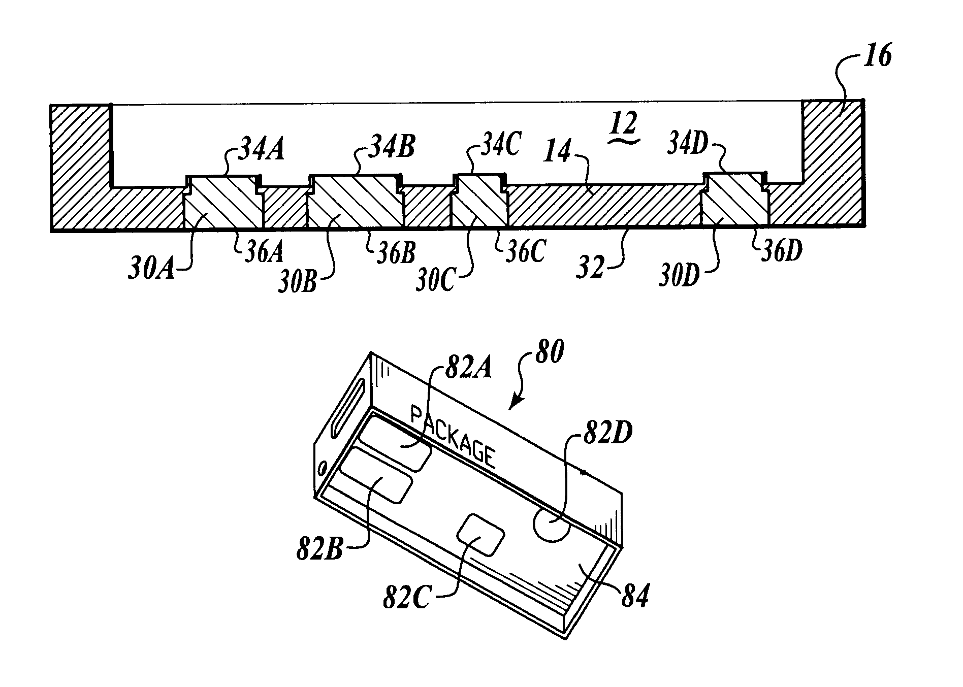
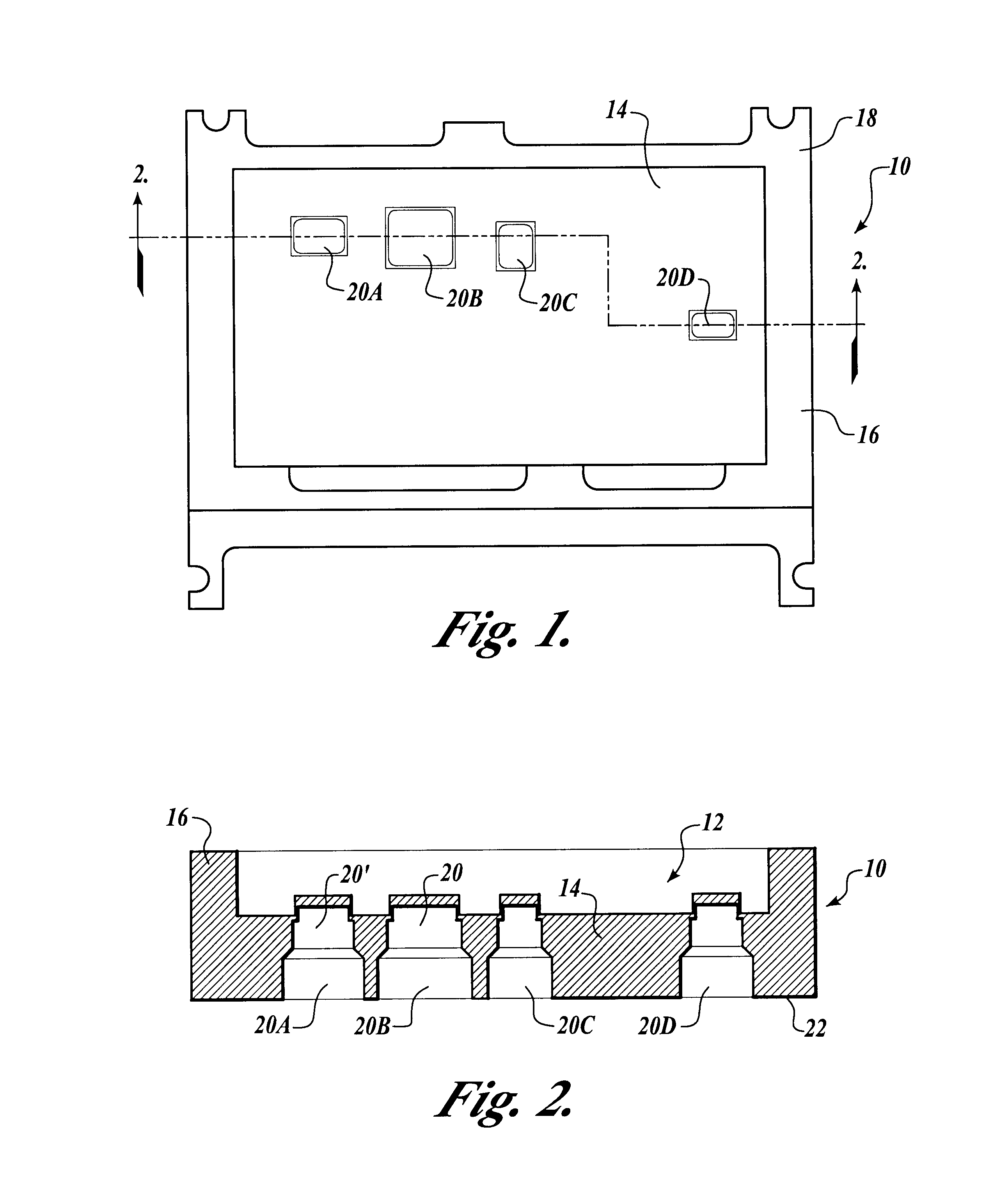
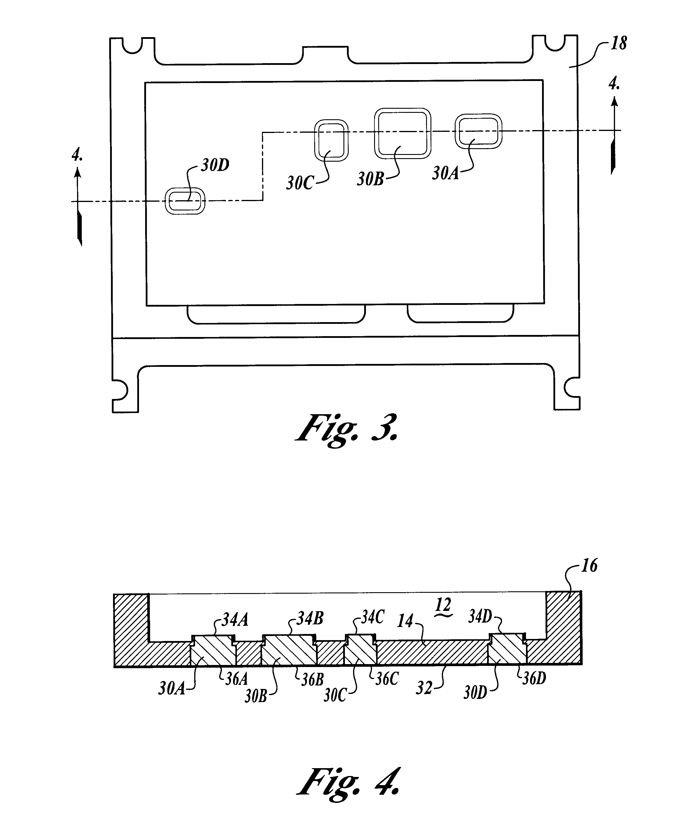
Electronics packages of the present invention are composed of a primary metallic component and one or more regions of a secondary material having thermal conductivity properties that are different from the thermal conductivity properties of the electronics package. A metallic component of the primary electronics package material is metallurgically compatible with a metallic component of the secondary material, such that a metallurgical bond may be formed between the electronics package and the secondary region(s). The CTE of the secondary material generally matches the CTE of the primary metallic material of the package. The secondary region(s) are arranged to provide one or more heat sinks in the electronics package, providing for dissipation of heat from a heat source on an electronic device mounted within the electronics package. Secondary regions may alternatively or additionally may be arranged to provide one or more area(s) for mounting electronic components such as ceramic ch...


PUM

PropertyMeasurementUnit
temperatureaaaaaaaaaa
particle sizesaaaaaaaaaa

Abstract

Electronics packages having a primary metallic material, such as a titanium metallic material, metallurgically bonded to one or more secondary regions within the primary metallic material, the composite regions having desirable thermal conductivity properties and having a coefficient of thermal expansion ("CTE") that generally matches the CTE of the primary metallic material are provided. Electronics packages comprising titanium having heat sinks comprising a metal matrix material such as aluminum silicon carbide or a composite metallic structure such as titanium aluminide/copper, are described. Methods for manufacturing electronics packages having a composite structure are also disclosed.

Description

The present invention relates to hermetic electronics packages constructed from a primary metallic material and having one or more secondary regions composed of material having disparate physical and / or structural properties. More specifically, electronics packages are provided with one or more regions of a secondary material having a high thermal conductivity and a coefficient of thermal expansion (CTE) that generally matches the CTE of the primary metallic material. In one embodiment, the electronics package comprises a primary metallic titanium component metallurgically bonded to a secondary metal matrix material, such as aluminum silicon carbide.Electronic components are used in countless applications in a wide variety of environments. Such components are subject to faulty operation, degradation and corrosion resulting from contact with dust, water vapor, gases, and the like, as well as from high IC) temperature and / or pressure conditions. Such components are, therefore, general...

Claims


Application Information

Patent Timeline
Patent Type & Authority Patents(United States)
IPC IPC(8): H01L23/34H01L23/373H05K7/20H01L23/367
CPCH01L23/3675H01L23/3677H05K7/20445H01L2924/09701Y10T428/12736Y10T428/12826Y10T428/12806Y10T428/12486H01L2924/0002H01L2924/00
Inventor JONES, HERMAN L.TAYLOR, EDWARD A.
Owner PACIFIC AEROSPACE & ELECTRONICS
Why Eureka
Try Eureka