Organic Light-Emitting Diode Device and Method for Producing Same

a light-emitting diode and organic technology, applied in the field of display, can solve the problems of imbalance and degradation of device efficiency, difficulty in adjusting device performance, and adjustment approach disadvantages

Inactive Publication Date: 2016-08-18
EVERDISPLAY OPTRONICS (SHANGHAI) CO LTD
View PDF6 Cites 6 Cited by
  • Summary
  • Abstract
  • Description
  • Claims
  • Application Information

AI Technical Summary

Benefits of technology

[0004]An objective of the present invention is to overcome the disadvantages of the conventional technology by providing an organic light-emitting diode device and a method for producing the organic light-emitting diode device, such that the problem of degradation of the efficiency of the device resulting from the change in the electrical properties during adjustment of the optical length of the conventional device can be solved.

Problems solved by technology

However, such an adjustment approach has disadvantages.
Specifically, since the organic material has a low carrier mobility, the driving voltage of the OLED device changes when the thickness of the organic material changes, such that the electrical properties of the device also change, which results in difficulties in adjustment of the performances of the device.
In a case that the cavity length is adjusted by adjusting the thickness of only one layer, the number of the holes and electrons of the OLED device also change, leading to imbalance and degradation of the efficiency of the device.

Method used


Image

  • Organic Light-Emitting Diode Device and Method for Producing Same
  • Organic Light-Emitting Diode Device and Method for Producing Same
  • Organic Light-Emitting Diode Device and Method for Producing Same

Examples


Embodiment Construction

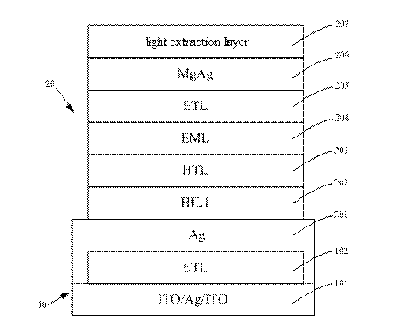
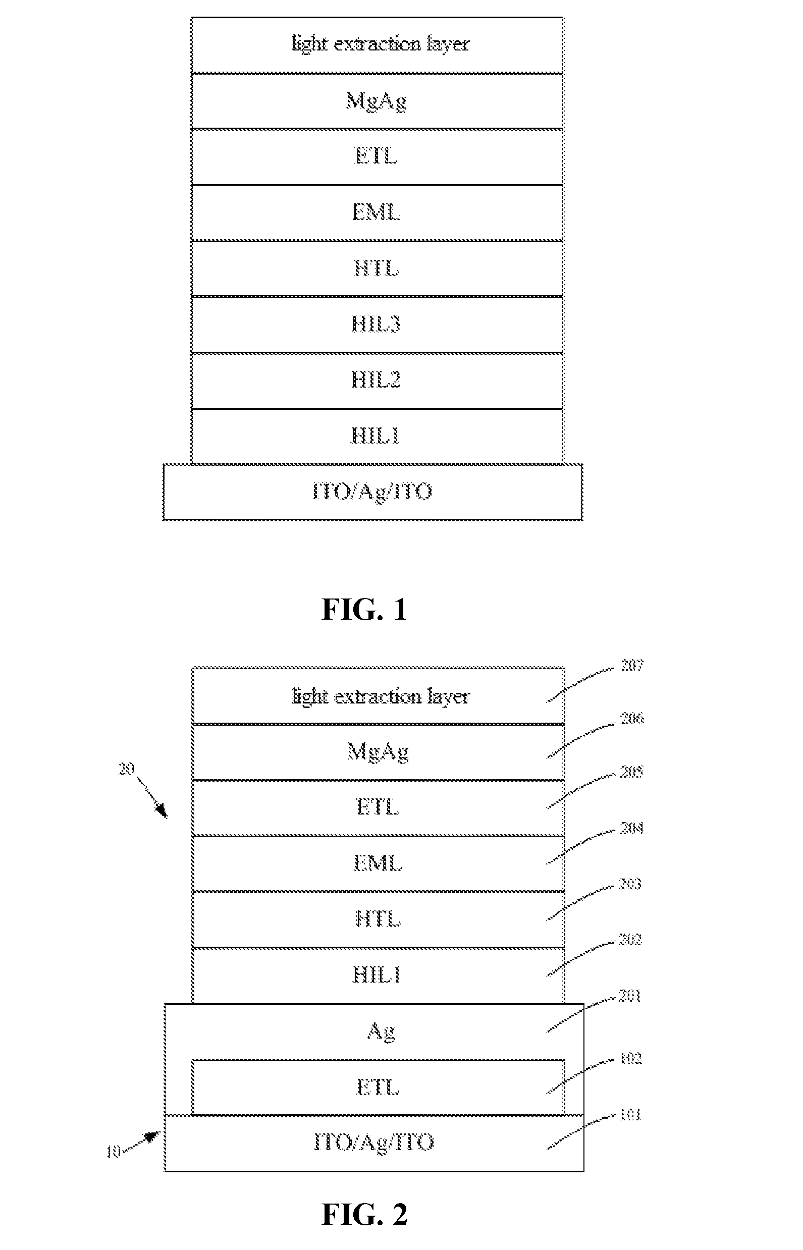
[0027]FIG. 2 is a diagrammatic view of an organic light-emitting diode device according to the present invention. The organic light-emitting diode device includes a separate design of an optical structure and an electrical structure. The electrical design includes a reflective layer and a cavity length adjustment layer. The electrical structure includes an anode connected to the reflective layer of the optical structure to provide current conduction between the optical structure and the electrical structure. By using the above design, adjustment of the optical length of the device can be achieved by adjusting the thickness of the cavity length adjustment layer, such that the device has a better optical effect and such that the optical properties of the device can be in the best status, Since the optical structure is separate from the electrical structure, the electrical properties of the device are not affected by the adjustment of the optical length, and the electrical structure ca...


PUM


Abstract

An organic light-emitting diode device includes an optical structure and an electrical structure. The optical structure includes a cavity length adjustment layer disposed on a reflective layer. The electrical structure includes an anode layer, a hole injection layer, a hole transport layer, a luminescent layer, an electron transport layer, and a cathode layer, which are disposed on the cavity length adjustment layer in sequence. The anode layer is electrically connected to the reflective layer. A method for producing an organic light-emitting diode device includes disposing a cavity length adjustment layer on a reflective layer to form an optical structure. An anode layer, a hole injection layer, a hole transport layer, a luminescent layer, an electron transport layer, and a cathode layer are disposed on the cavity length adjustment layer in sequence to form an electrical structure. The anode layer is electrically connected to the reflective layer.

Description

BACKGROUND OF THE INVENTION[0001]The present invention relates to the display field and, more particularly, to an organic light-emitting diode device and a method for producing the organic light-emitting diode device.[0002]Organic light-emitting diodes (also known as organic electroluminescence) include the features of self-illumination and use a very thin coating of organic material and a very thin glass substrate. The organic material emits light when electric current passes through.[0003]Conventional organic light-emitting didoes (OLEDs) use top emission and adjust the chromaticity and the light intensity of the color emitted by the display panel through adjustment of the microcavity structure, obtaining a better chromaticity coordinate value. FIG. 1 shows a conventional OLED device structure. A first hole injection layer (HTL1), a second hole injection layer (HTL2), a third hole injection layer (HTL3), a hole transport layer (HTL), an emissive layer (EML), an electron transport ...

Claims


Application Information

Patent Timeline
Patent Type & Authority Applications(United States)
IPC IPC(8): H01L51/52H01L51/56H01L51/50
CPCH01L51/5275H01L51/5271H01L2251/53H01L51/56H01L51/5088H10K50/852H10K71/00H10K2102/351
Inventor HE, ZHIJIANGGAO, YANPIN
Owner EVERDISPLAY OPTRONICS (SHANGHAI) CO LTD
Why Eureka
Try Eureka