
Array substrate and display device

a technology which is applied in the field of array substrate and display device, can solve the problems of complex manufacturing process of array substrate in the prior ar

Active Publication Date: 2016-08-25
SHENZHEN CHINA STAR OPTOELECTRONICS TECH CO LTD
View PDF3 Cites 18 Cited by
  • Summary
  • Abstract
  • Description
  • Claims
  • Application Information

AI Technical Summary

Benefits of technology

The present invention is about solving the problem of interference between the left and right eyes when watching 3D displays. It provides a 3D glasses, curved surface display device and 3D display device that can improve the viewing experience. Additionally, the invention provides an array substrate that allows for the formation of address lines without affecting the arrangement of scan lines and data lines, which simplifies the manufacturing process. This results in improved manufacturing efficiency and cost-effectiveness.

Problems solved by technology

In the process of implementing the present disclosure, the inventor found that the prior arts suffer from at least the following problems: in an in-cell liquid crystal display device, at least structures such as address lines and corresponding insulation layers are needed; and in the manufacturing process of array substrates, at least one photo engraving process (PEP) is needed.
It is therefore concluded that the manufacturing process of array substrates is too complex in the prior arts.

Method used


Image

  • Array substrate and display device
  • Array substrate and display device
  • Array substrate and display device

Examples


embodiment 1

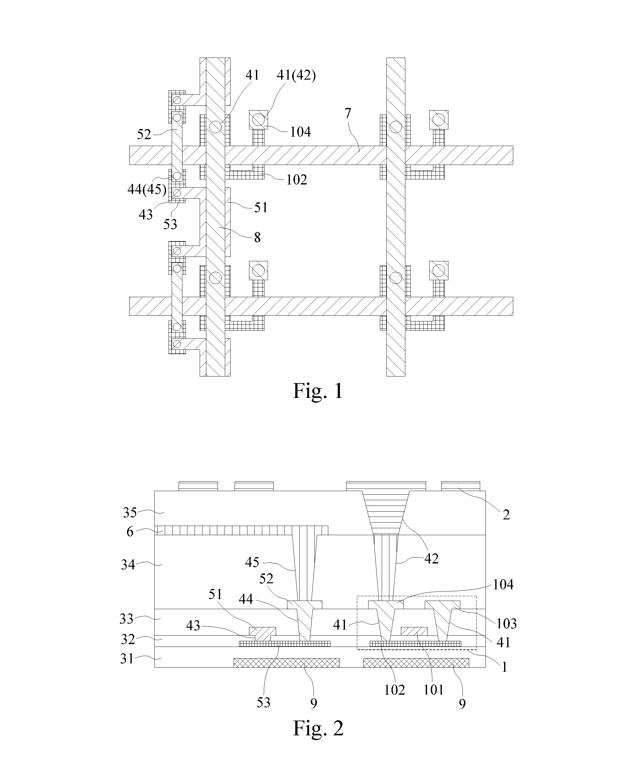
[0027]As shown in FIGS. 1 and 2, the present embodiment provides an array substrate comprising a plurality of pixel units, each having a thin film transistor (TFT) 1 and a pixel electrode 2.

[0028]In the present embodiment, the TFT 1 is in the form of a top-gate TFT. Preferably, the present embodiment adopts a low temperature poly-silicon (LTPS) to form a channel of the TFT 1. Compared with traditional amorphous silicon (a-Si), the LTPS has a higher carrier mobility, and therefore can achieve a higher resolution and lower power consumption, as well as a higher integration of devices on the array substrate.

[0029]In the present embodiment, a gate 101 is located above a LTPS 102, with an insulating layer 32 arranged therebetween. An insulating layer 33 is arranged above the gate 101, and is provided thereon with a source 103 and a drain 104 which are connected to the LTPS 102 through a via hole 41. A pixel electrode 2 and the drain 104 are connected to each other through a via hole 42 w...

embodiment 2

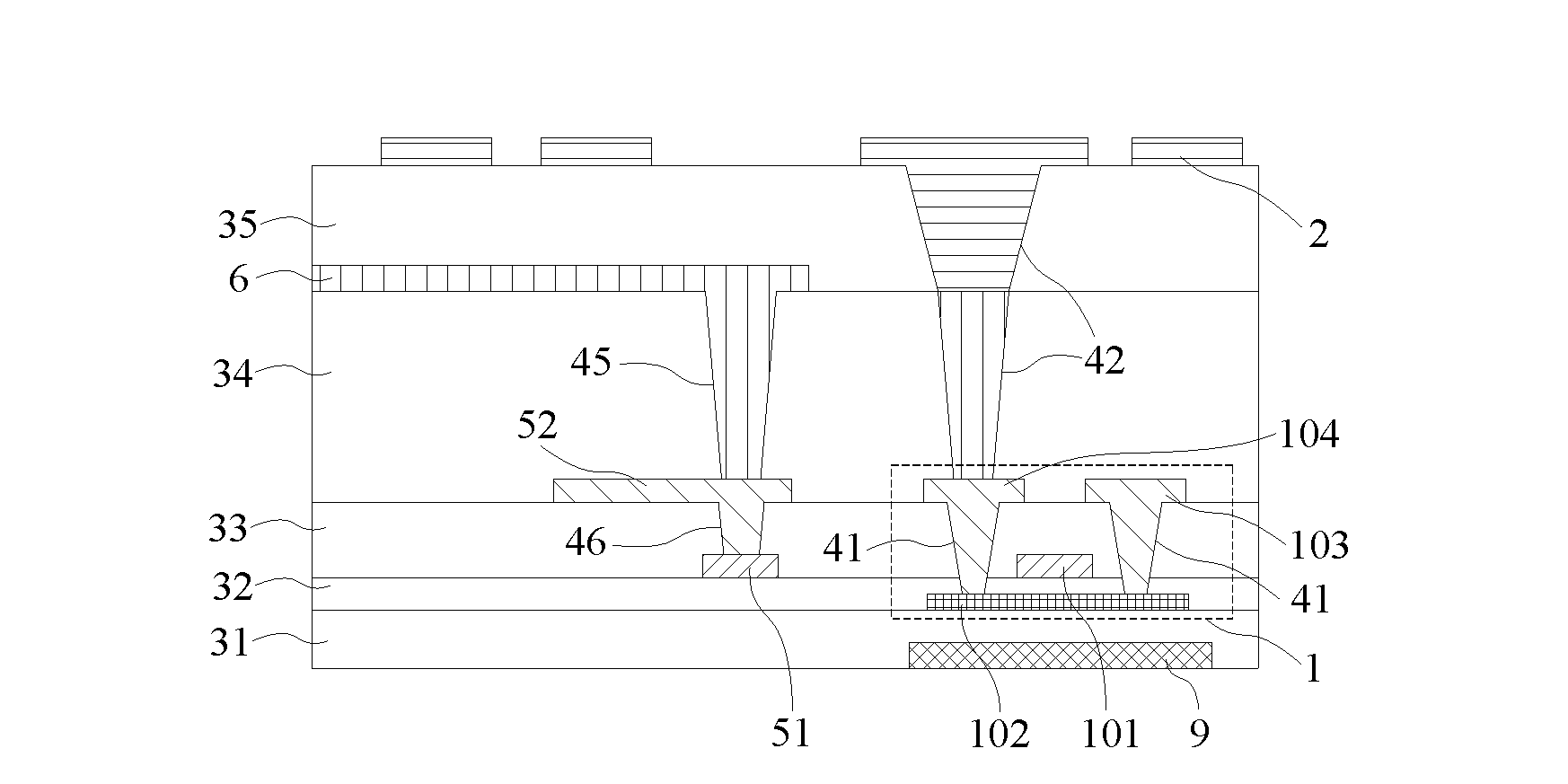
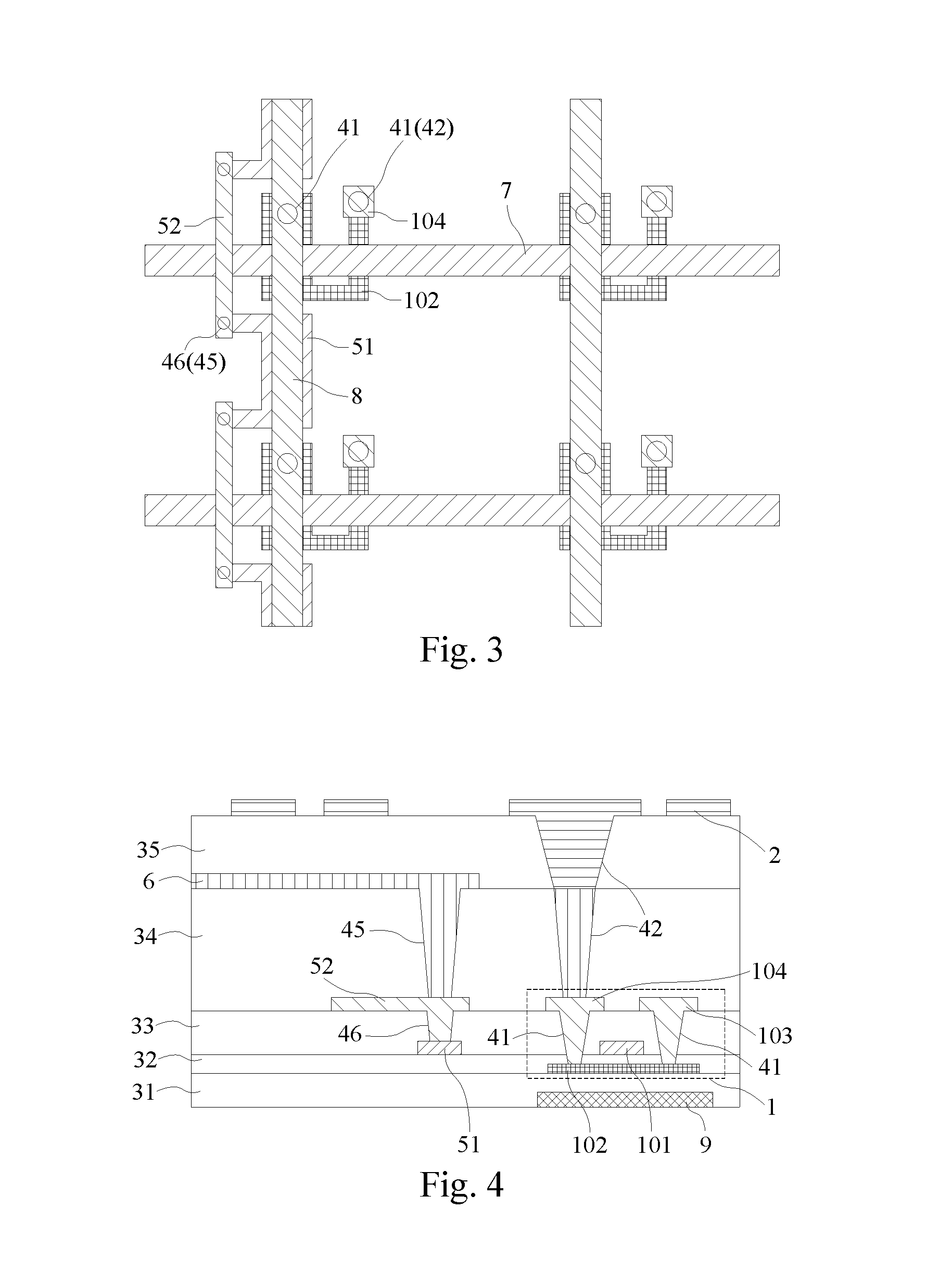
[0038]As shown is FIGS. 3 and 4, the present embodiment is basically the same as embodiment 1. The difference is that, in the present embodiment, the first metal wire 51 and the second metal wire 52 are connected to each other directly through a via hole 46 which runs through the insulating layer 33.

[0039]Compared with embodiment 1, the connecting piece and the light shielding layer thereunder can be omitted in the present embodiment. In addition, the address line according to the present embodiment is formed entirely by connecting the first metal wire 51 and the second metal wire 52, i.e. the address line is formed entirely by a metal material, which renders the touch signal transmitted in the address lines more stable and more reliable.

embodiment 3

[0040]The present disclosure provides a display device, which can be the display device for cell phones, tablet PCs, and the like with touch function, and achieves touch circuits by means of in-cell technology. The display device comprises a color filter substrate, and the array substrate according to embodiment 1 or embodiment 2.

[0041]The display device is preferably a fringe field switching (FFS) liquid crystal display device, and the core technical features thereof are: through the electric field generated at the edge of the slit-shaped pixel electrodes within a same plane, to cause the plane rotation of all the orientated liquid crystal molecules among slit-shaped electrodes and right above electrodes, thereby improving the light transparency of the liquid crystal layer. The FFS technology can improve the quality of pictures displayed on the liquid crystal display device, and make the liquid crystal display device have such advantages as high resolution, high transparency, low p...


PUM


Abstract

Disclosed are an array substrate and a display device which belong to the technical field of displays, and solve the technical problem that, in the existing in-cell technology, the manufacturing process of array substrates is too complex. The array substrate comprises a plurality of pixel units each having a thin film transistor, a plurality of common electrodes, and a plurality of address lines. The address lines each are formed by connecting a first metal wire and a second metal wire, the first metal wire being located at a same layer as a gate of the thin film transistor, and the second metal wire being located at a same layer as a source and a drain of the thin film transistor.

Description

[0001]The present application claims benefit of Chinese patent application CN201410804969.4, entitled “Array substrate and display device” and filed on Dec. 19, 2014, the entirety of which is incorporated herein by reference.TECHNICAL FIELD[0002]The present disclosure relates to the technical field of displays, and in particular, to an array substrate and a display device.TECHNICAL BACKGROUND[0003]With the development of display technology, liquid crystal display devices have become the most common display devices.[0004]In the meanwhile, with the popularization of smart electronic products, capacitive touch screens are also widely used in electronic products, such as cell phones, tablet PCs, etc. Currently, capacitive touch screens mainly use one glass solution (OGS), on-cell, and in-cell technologies. Compared with OGS and on-cell technologies, in-cell technology is superior in production process, and products using it are thinner and lighter, more transparent, and more stable in s...

Claims


Application Information

Patent Timeline
IPC IPC(8): G06F3/041H04N13/04G06F3/044
CPCG02F1/1343G02F1/1362G02F1/1368G06F3/0412H04N13/0429G06F3/044G06F2203/04103G06F2203/04107G06F3/0416G02F1/13338G02F1/134309G02F1/136286G02F1/134318G02F1/136209H04N13/332
Inventor MING, XINGSHEN, ZHIYUAN
Owner SHENZHEN CHINA STAR OPTOELECTRONICS TECH CO LTD
Learn More