Semiconductor Device and Manufacturing Method Thereof

a semiconductor and semiconductor technology, applied in the direction of semiconductor devices, electrical devices, transistors, etc., can solve the problems of electrical characteristics deterioration of transistors, and achieve the effects of reducing the area of the driver circuit, suppressing deterioration, and reducing the width of the channel

Inactive Publication Date: 2016-09-22
SEMICON ENERGY LAB CO LTD
View PDF30 Cites 1 Cited by
  • Summary
  • Abstract
  • Description
  • Claims
  • Application Information

AI Technical Summary

Benefits of technology

[0045]Furthermore, in an active matrix organic EL display device, a transistor used as a constant current source has the s-channel structure, whereby the deterioration can be suppressed; thus, the structure is a particularly effective structure.
[0046]Furthermore, when a transistor used in a driver circuit of an active matrix display device has the s-channel structure, the channel width W can be reduced, so that the area of the driver circuit can be reduced. For example, the width of the driver circuit is reduced to 0.5 mm, preferably 0.3 mm, and a narrower frame width can be achieved.
[0047]With the s-channel structure, high electrical characteristics (such as a high on-state current value) and a highly reliable semiconductor device can be achieved. The high on-state current value can achieve a further decrease in channel width (W). A highly integrated semiconductor device can be provided. A semiconductor device which can operate at high speed can be provided. With the s-channel structure, an excellent S value can be obtained. A semiconductor device with low power consumption can be provided. A semiconductor device with high productivity can be provided. A semiconductor device with high yield can be provided. A noble semiconductor device can be provided. A module including any of the above semiconductor devices can be provided. An electronic device including any of the above semiconductor devices or the module can be provided.

Problems solved by technology

However, it is known that miniaturization of a transistor causes deterioration of electrical characteristics of the transistor.

Method used


Image

  • Semiconductor Device and Manufacturing Method Thereof
  • Semiconductor Device and Manufacturing Method Thereof
  • Semiconductor Device and Manufacturing Method Thereof

Examples


embodiment 1

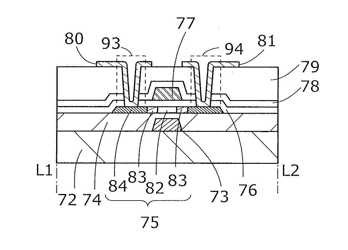
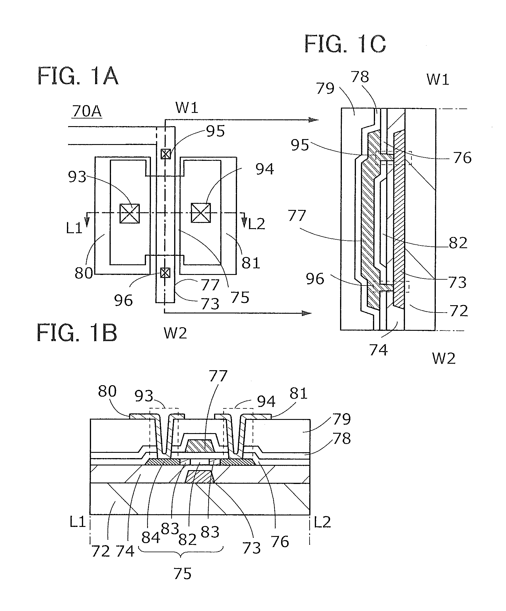
[0078]FIG. 1B is a cross-sectional view (in a channel length direction) of an example of an n-channel transistor 70A including a thin polysilicon film, which is one embodiment of the present invention. FIG. 1A is a top view of the transistor 70A and FIG. 1C is a cross-sectional view of the transistor 70A in a channel width W direction.

[0079]The transistor 70A includes, over a substrate 72 having an insulating surface, a conductive film 73 functioning as a gate, an insulating film 74 over the conductive film 73, a semiconductor film 75 overlapping with the conductive film 73 with the insulating film 74 provided therebetween, an insulating film 76 over the semiconductor film 75, a conductive film 77 overlapping with the semiconductor film 75 with the insulating film 76 provided therebetween and functioning as a gate, an insulating film 78 over the conductive film 77, an insulating film 79 over the insulating film 78, and a conductive film 80 and a conductive film 81 which are electric...

embodiment 2

[0111]In this embodiment, an example where an n-channel transistor 70 and a p-channel transistor 71 are provided over the same substrate is shown. When the n-channel transistor 70 and the p-channel transistor 71 are combined, a CMOS circuit or the like can be fabricated.

[0112]FIGS. 6A and 6B are cross-sectional views of transistors each including a thin silicon film, which can be used in the display device of one embodiment of the present invention. FIGS. 6A and 6B show n-channel transistors 70 and p-channel transistors 71.

[0113]The transistor 70 includes, over a substrate 72 having an insulating surface, a conductive film 73 functioning as a gate, an insulating film 74 over the conductive film 73, a semiconductor film 75 overlapping with the conductive film 73 with the insulating film 74 provided therebetween, an insulating film 76 over the semiconductor film 75, conductive films 77a and 77b overlapping with the semiconductor film 75 with the insulating film 76 provided therebetwee...

embodiment 3

[0120]In this embodiment, cross-sectional views of transistors each including a back gate electrode, which are shown in FIGS. 1A to 1C, FIGS. 2A to 2C, FIGS. 3A to 3C, FIGS. 4A to 4C, FIGS. 5A to 5C, and FIGS. 6A and 6B, and a pixel electrode provided over the transistors is illustrated to show an example of a fabrication process thereof. Although FIGS. 7A to 7E, FIGS. 8A to 8D, and FIGS. 9A and 9B show a process of fabricating a p-channel transistor and an n-channel transistor over a substrate as an example, in the case where a circuit is configured by transistors having the same conductivity, the process of fabricating either one of the transistors is used.

[0121]First, a conductive film 502 functioning as a back gate electrode is formed on an insulating surface of a substrate 501 as shown in FIG. 7A. The conductive film 502 can be formed using a conductive material containing one or more selected from Al, W, Mo, Ti, and Ta. Although tungsten is used for the conductive film 502 in ...


PUM


Abstract

An object is to achieve high electrical characteristics (a high on-state current value, an excellent S value, and the like) and a highly reliable semiconductor device. A high on-state current value is achieved, whereby a further reduction in channel width (W) is achieved. A second conductive layer functioning as a gate electrode has a function of electrically surrounding side surfaces of a semiconductor film in a cross section in a channel width direction. With this structure, on-state current of a transistor can be increased. To achieve a semiconductor device with less hot-carrier degradation, the gate electrode has a tapered portion.

Description

BACKGROUND OF THE INVENTION[0001]1. Field of the Invention[0002]The present invention relates to, for example, a transistor, a semiconductor device, and manufacturing methods thereof. The present invention relates to, for example, a display device, a light-emitting device, a lighting device, a power storage device, a memory device, a processor, and an electronic device. The present invention relates to a method for manufacturing a display device, a liquid crystal display device, a light-emitting device, a memory device, and an electronic device. The present invention relates to a driving method of a semiconductor device, a display device, a liquid crystal display device, a light-emitting device, a memory device, and an electronic device.[0003]Note that one embodiment of the present invention is not limited to the above technical field. The technical field of one embodiment of the invention disclosed in this specification and the like relates to an object, a method, or a manufacturin...

Claims


Application Information

Patent Timeline
Patent Type & Authority Applications(United States)
IPC IPC(8): H01L29/786H01L29/45
CPCH01L29/78696H01L29/458H01L29/78654H01L29/78672H01L21/3221H01L29/42384H01L29/42392H01L29/78627H01L29/78633H01L29/78648
Inventor YAMAZAKI, SHUNPEI
Owner SEMICON ENERGY LAB CO LTD
Why Eureka
Try Eureka