Semiconductor device

Active Publication Date: 2016-10-06
SHARP KK
View PDF2 Cites 4 Cited by
  • Summary
  • Abstract
  • Description
  • Claims
  • Application Information

AI Technical Summary

Benefits of technology

[0026]According to one embodiment of the present invention, in a semiconductor device including a memory transistor which includes a metal oxide layer as the active layer and which utilizes transition from a semiconductor state to a resistor state, melting of the drain ele

Problems solved by technology

In this memory transistor, the metal oxide semiconductor is a resistor after

Method used


Image

  • Semiconductor device
  • Semiconductor device
  • Semiconductor device

Examples


first embodiment

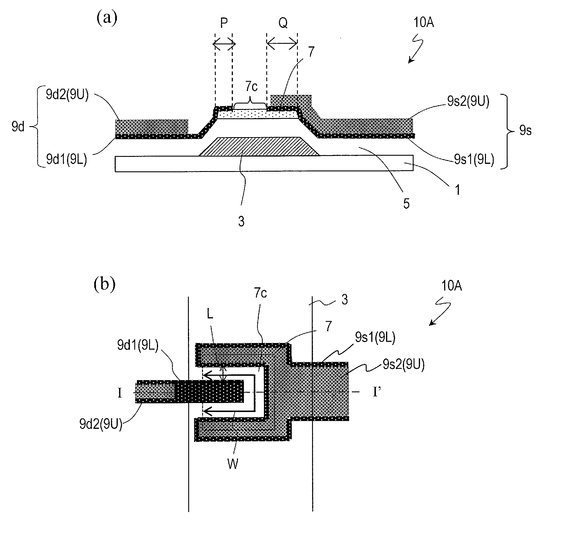
[0068]FIG. 1(a) is a cross-sectional view showing a memory transistor 10A in a semiconductor device of the present embodiment. FIG. 1(b) is a plan view of the memory transistor 10A. FIG. 1(a) shows a cross-sectional structure taken along line I-I′ of FIG. 1(b).

[0069]The semiconductor device of the present embodiment includes a substrate 1 and a memory transistor 10A supported on the substrate 1. The memory transistor 10A is, for example, an n-channel type memory transistor.

[0070]The memory transistor 10A includes a gate electrode 3, an active layer 7 including a metal oxide (hereinafter, “metal oxide layer”), a gate insulating film 5 interposed between the gate electrode 3 and the metal oxide layer 7, and a source electrode 9s and a drain electrode 9d electrically connected with the metal oxide layer 7. When viewed in a direction normal to the substrate 1, at least part of the metal oxide layer 7 is arranged so as to extend over the gate electrode 3 with the gate insulating film 5 i...

examples

[0101]Here, memory transistors 10(1), 10(2) of an inventive example and a reference example were manufactured and compared as to damage to the memory transistors due to writing.

[0102]FIGS. 3(a) and 3(b) are a cross-sectional view and plan view of the memory transistor 10(1) of the inventive example. The memory transistor 10(1) is different from the memory transistor 10A shown in FIG. 1 in that the portion Q of the source electrode 9s which is present on the metal oxide layer 7 is formed only by the first source metal layer 9s1, and the second source metal layer 9s2 is not provided on the metal oxide layer 7. The other components are the same as those of the memory transistor 10A. In the memory transistor 10(1), a Ti layer was formed as the first drain metal layer 9d1 and the first source metal layer 9s1, an Al layer was formed as the second drain metal layer 9d2 and the second source metal layer 9s2, and an In—Ga—Zn—O based semiconductor layer was formed as the metal oxide layer 7. ...

second embodiment

[0179]Hereinafter, the second embodiment of the semiconductor device of the present invention is described. The semiconductor device of the present embodiment is different from the semiconductor device of the first embodiment in that it includes a memory transistor which has a protection layer as the etch stop on the metal oxide layer. The other components are the same.

[0180]FIGS. 22(a) and 22(b) are a plan view and cross-sectional view showing an example of the configuration of a memory transistor 10C in the second embodiment. The cross section shown in FIG. 22(b) is a cross section taken along line A-A′ of FIG. 22(a). In FIG. 22, elements which are equivalent to those of FIG. 1 are designated by the same reference numerals, and descriptions thereof are herein omitted.

[0181]The memory transistor 10C includes a protection layer 31 provided between the metal oxide layer 7 and the source wire layer. The protection layer 31 is in contact with at least the channel region 7c of the metal...


PUM


Abstract

A semiconductor device includes a memory transistor (10A) which is capable of being irreversibly changed from a semiconductor state where drain current Ids depends on gate voltage Vg to a resistor state where drain current Ids does not depend on gate voltage Vg. The memory transistor (10A) includes a gate electrode (3), a metal oxide layer (7), a gate insulating film (5), and source and drain electrodes. The drain electrode (9d) has a multilayer structure which includes a first drain metal layer (9d1) and a second drain metal layer (9d2), the first drain metal layer (9d1) being made of a first metal whose melting point is not less than 1200° C., the second drain metal layer (9d2) being made of a second metal whose melting point is lower than that of the first metal. Part P of the drain electrode 9d extends over both the metal oxide layer (7) and the gate electrode (3) when viewed in a direction normal to a surface of the substrate. The part (P) of the drain electrode (9d) includes the first drain metal layer (9d1) and does not include the second drain metal layer (9d2).

Description

TECHNICAL FIELD[0001]The present invention relates to a semiconductor device which includes a memory transistor.BACKGROUND ART[0002]Using an element which has a transistor structure (hereinafter, referred to as “memory transistor”) as a memory element which can be used as a ROM (read only memory) has been conventionally proposed.[0003]For example, Patent Document 1 discloses a nonvolatile memory transistor which has a MOS transistor structure. In this memory transistor, a high electric field is applied to a gate insulating film so as to cause a dielectric breakdown, whereby writing is realized. Patent Document 2 discloses a memory transistor which utilizes a variation in threshold voltage which can be caused by application of a predetermined writing voltage to a gate.[0004]On the other hand, Patent Document 3 of the present applicant proposes a novel nonvolatile memory transistor which is capable of reducing the power consumption as compared with conventional nonvolatile memory tran...

Claims


Application Information

Patent Timeline
IPC IPC(8): H01L27/112G02F1/1368H01L27/12G09G3/36H01L29/786H01L29/417
CPCH01L27/11206H01L29/7869H01L29/41733G09G2300/0426G09G3/3655G02F1/1368G09G2300/0842H01L27/1225H01L27/101H01L29/45H01L27/1255H10B20/20H01L27/1251H01L29/78678G09G2300/08
Inventor KATOH, SUMIOUEDA, NAOKI
Owner SHARP KK
Why Eureka
Try Eureka