Light Emitting Module

a technology of light-emitting modules and modules, applied in the direction of basic electric elements, electrical apparatus, semiconductor devices, etc., can solve the problems of poor reliability and complex manufacturing process, and achieve the effect of simple connection process and reliable connection

Inactive Publication Date: 2016-10-20
EVERLIGHT ELECTRONICS
View PDF13 Cites 12 Cited by
  • Summary
  • Abstract
  • Description
  • Claims
  • Application Information

AI Technical Summary

Benefits of technology

[0005]The present invention provides a light emitting module which makes the substrate connecting process simple and the connection reliable.
[0018]As can be known from the above descriptions, in the light emitting module according to one of the embodiments of the present invention, the electrode substrate comprises a first joint portion and an opposite second joint portion which are located at two opposite ends of the electrode substrate respectively. The first joint portion comprises a first through hole or a first notch. By applying present invention, the substrate connecting process is made simple and reliable because metal wires may be connected not through spot soldering which presents a risk of loose of the soldered point and thus leads to a poor reliability. In the light emitting module according to another embodiment of the present invention, the electrode substrate and the LEDs are covered by the fluorescent encapsulant and the upper encapsulant thickness is greater than the lower encapsulant thickness, so the light emitting module presents good light emission uniformity.

Problems solved by technology

However, this makes the manufacturing process complex, and the spot soldering presents a risk of loose of the soldered point, which leads to a poor reliability.

Method used


Image

  • Light Emitting Module
  • Light Emitting Module
  • Light Emitting Module

Examples


Embodiment Construction

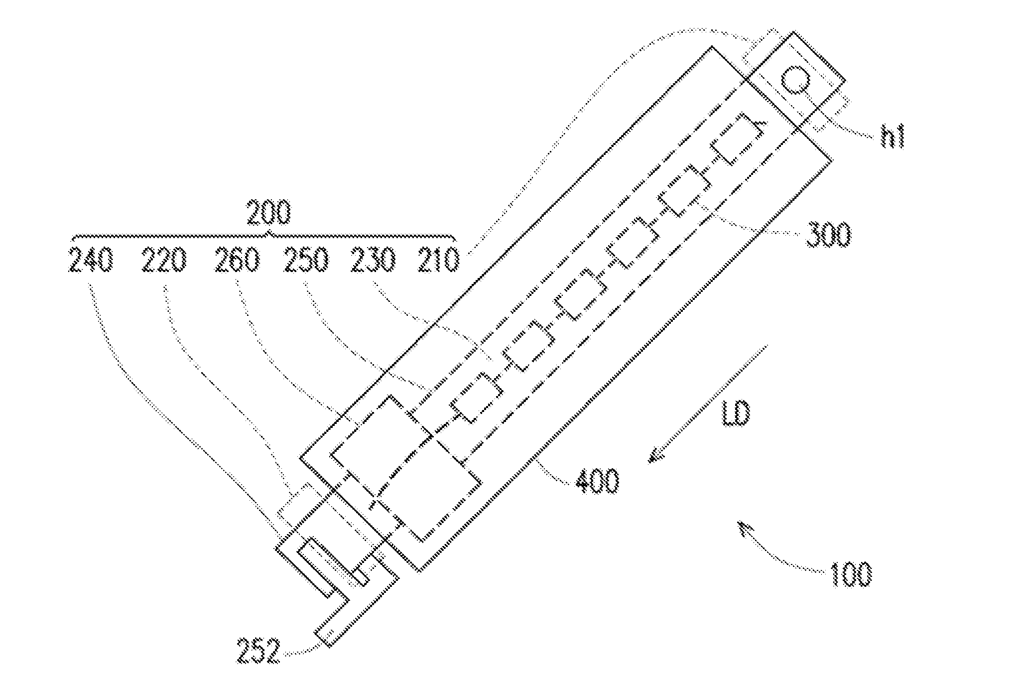
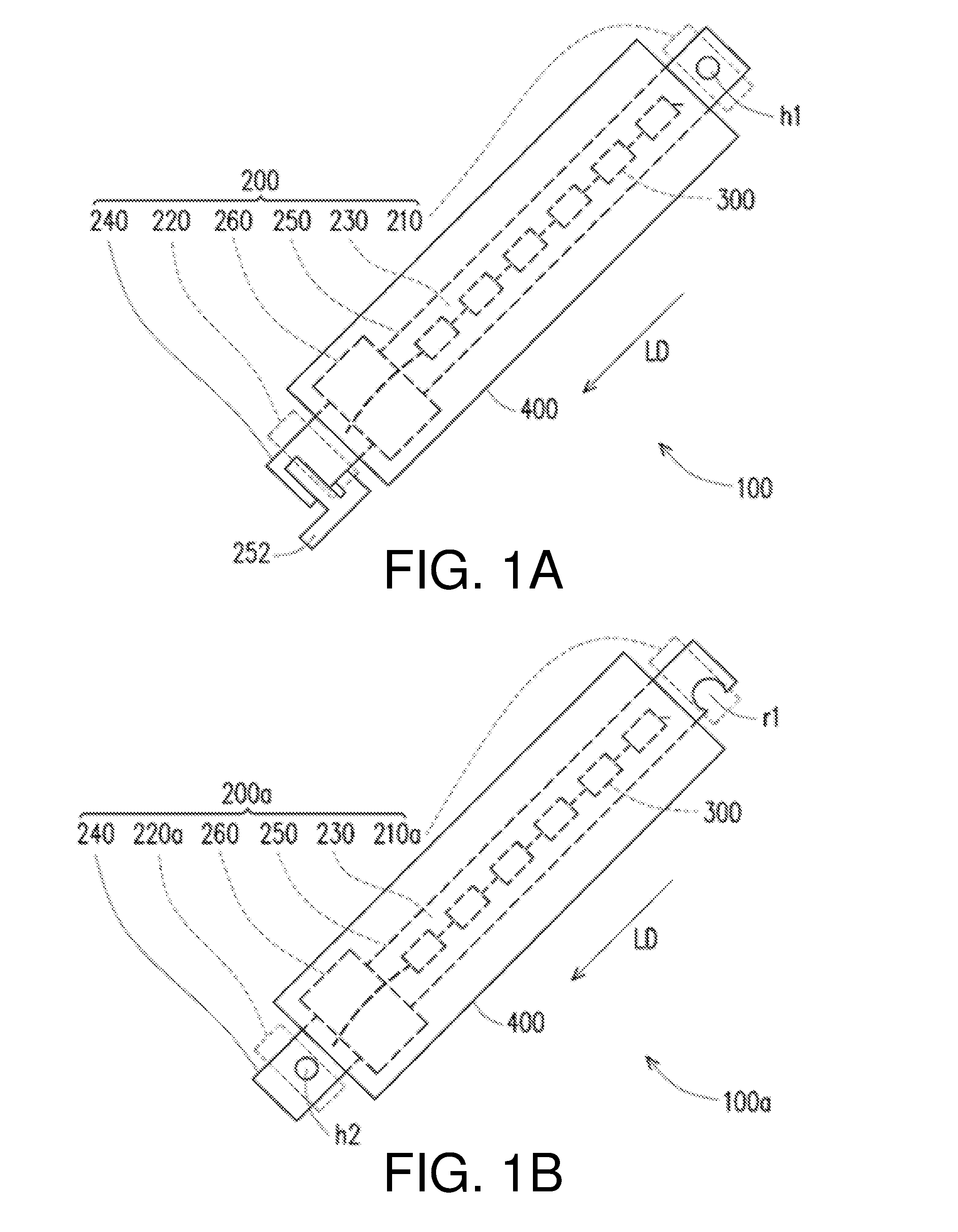
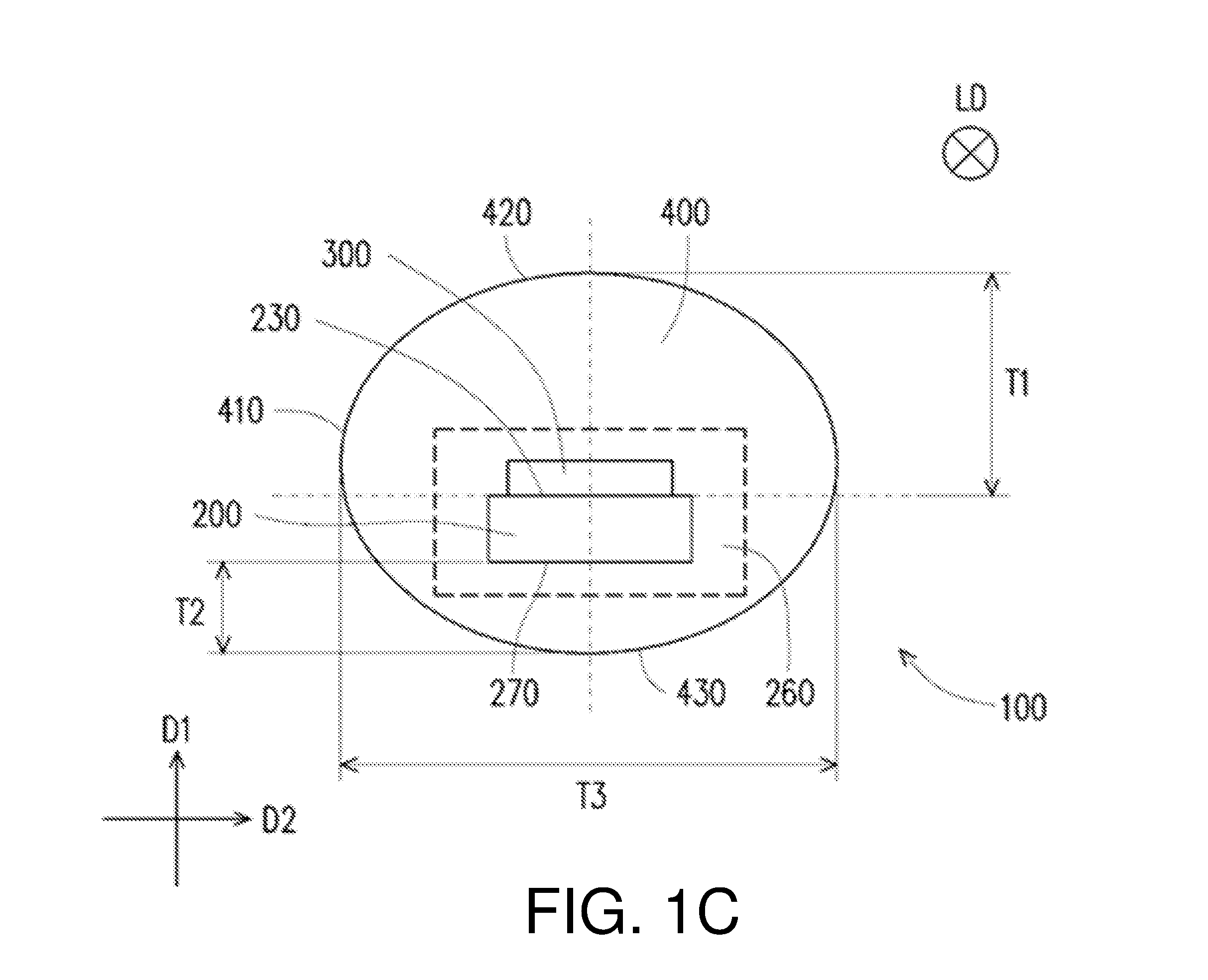
[0030]FIG. 1A is a schematic top view of a light emitting module according to an embodiment of the present invention. Referring to FIG. 1A, the light emitting module 100 in this embodiment comprises an electrode substrate 200 and a plurality of light-emitting diodes (LEDs) 300. The LEDs 300 can be, for example, HV-LED, DC-LED, OLED, III-V compound LED, LD, photonic Crystal LED, Hybrid LED, Nanorod LED, HP LED, or AC-LED. The LED die can be electrically connected via wire bonding, tape automated bonding or flip chip bonding. The LED die can be packaged as SMD type, DIP type, high power type, piranha type or without any package. The present invention is not limited thereto. The electrode substrate 200 comprises a first joint portion 210 and an opposite second joint portion 220 which are located at two opposite ends of the electrode substrate 200 respectively. The electrode substrate 200 is an electrically conductive substrate. The electrode substrate 200 is, for example, a metal elect...


PUM


Abstract

A light emitting module including an electrode substrate and a plurality of light emitting diodes is provided. The electrode substrate includes a carrying surface, and further includes a first joint portion and a second joint portion that are located at opposite ends of the electrode substrate respectively. The first joint portion includes a first through hole or a first notch. The plurality of light emitting diodes is disposed on the carrying surface of the electrode substrate, wherein the plurality of light emitting diodes is arranged along a long side direction of the electrode substrate, and is electrically coupled to the electrode substrate.

Description

CROSS-REFERENCES TO RELATED APPLICATIONS[0001]This application claims priority to Taiwan Patent Application No. 104112567, filed on Apr. 20, 2015, which is incorporated by reference in its entirety.TECHNICAL FIELD[0002]The present invention relates to a light emitting module.DESCRIPTIONS OF RELATED ART[0003]Owing to rapid development of the semiconductor technologies, currently light-emitting diodes (LEDs) can provide a high luminance output and be used in various light mixing applications. The LEDs operate in the following way: by applying a current to a compound semiconductor, electrons and holes are recombined so that energy is released in the form of light. Because the LEDs emit light not through heating or discharging, the LEDs have a long lifetime of more than one hundred thousands of hours. Moreover, as compared with the conventional incandescent light sources, the LEDs further have such advantages as power saving, a small volume, and a short response time, so they have been ...

Claims


Application Information

Patent Timeline
Patent Type & Authority Applications(United States)
IPC IPC(8): H01L25/075H01L33/56H01L33/54H01L27/15
CPCH01L25/0753H01L33/54H01L33/56H01L27/156H01L27/15H01L33/38H01L33/505
Inventor LIEN, YA-HUEICHANG, CHUNG-KAI
Owner EVERLIGHT ELECTRONICS
Why Eureka
Try Eureka