Apparatus and method for detecting high-energy radiation

a detector and high-energy technology, applied in the direction of radiation measurement, instruments, calibrators, etc., can solve the problems of not being able to accurately determine what type of radiation (spectroscopic information, radiation dose estimation,

Inactive Publication Date: 2016-10-27
RADIATION WATCH LTD
View PDF0 Cites 3 Cited by
  • Summary
  • Abstract
  • Description
  • Claims
  • Application Information

AI Technical Summary

Benefits of technology

[0034]The charge collection electrodes form a pixellated charge collection substrate forming a corresponding p

Problems solved by technology

It is not possible to achieve real-time monitoring and evaluation.
Although such inference can be drawn based on experience, nevertheless it is not possible to precisely determine what type of radiation (spectroscopic information) has been sensed nor an estimate of radiation dose which takes into account such information.
Additionally, known passive detection systems generally have poor sensitivity to ionising radiation.
However, silicon has poor sensitivity to ionising radiation since it does not have a high atomic number (Z), therefore there is inefficient conversion of the incident radiation to electric current and devices using such technology suffer from poor signal to noise ratio.
Another drawback of known active detectors i

Method used


Image

  • Apparatus and method for detecting high-energy radiation
  • Apparatus and method for detecting high-energy radiation
  • Apparatus and method for detecting high-energy radiation

Examples


Embodiment Construction

Detector Substrate

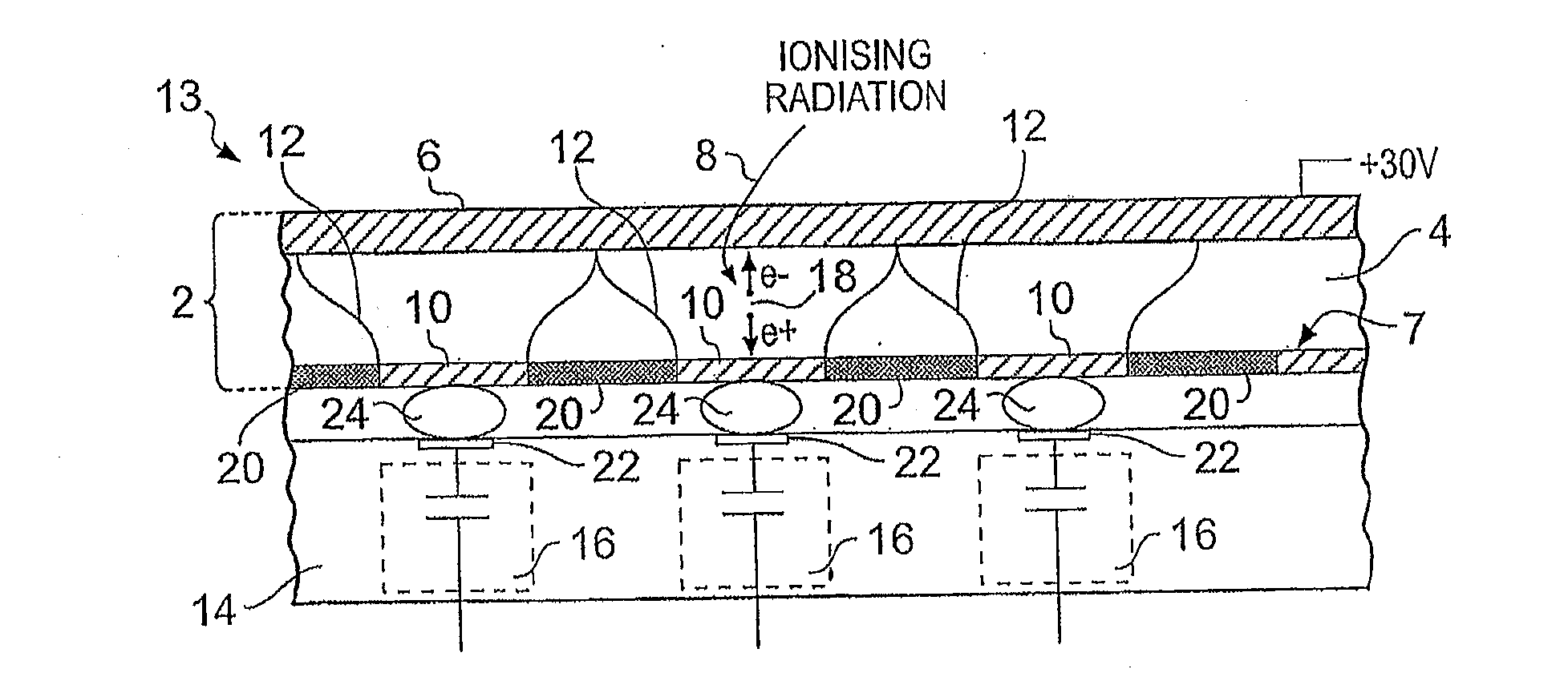
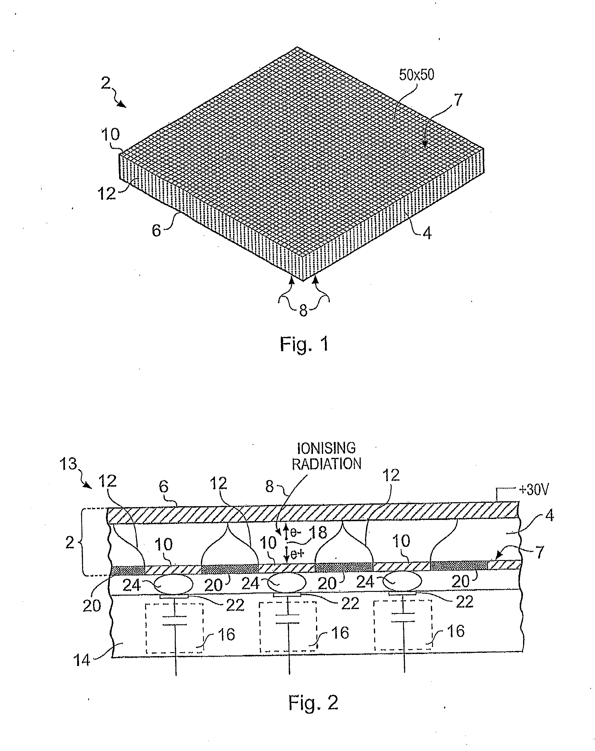
[0055]A detector substrate 2 in accordance with an embodiment of the present invention has a semi-conductor crystal 4 clad on one surface thereof with a plurality of conductive contact pads 10 which may act as charge collection electrodes and on an opposing side surface clad with a layer of conductive material 6 for forming a biasing electrode. The array of contact pads forms a pixellated surface 7.

[0056]In the illustrated example the semi-conductor crystal 4 is CdTe but other suitable semi-conductor materials may be used, such as CZT, Si, GaAs, CdMgTe or a halide-metal compound with a high atomic number, by way of non-limiting example.

[0057]Each conductive pad 10 is electrically isolated from the other contact pads. The array of pads 10 forms an array of ionising radiation sense volumes 12. In the illustrated example an array of 50×50 sense volumes 12 is created from the array of conductive contact pads, each pad having dimensions 100 microns by 100 microns. Typic...


PUM


Abstract

An apparatus for spatially correcting an image frame is disclosed. In some embodiments, the apparatus stores a frame of pixel values and scans a multi-pixel correction window across the frame. Spatial correction is performed on pixels within the window at correction positions during the scan. The spatial correction comprises estimating pixel values at value estimation positions based on one or more pixel values within the window for pixels satisfying a logical condition. The value estimation positions correspond to pixel values which do not fall within the window again during the scan. Further disclosed is an apparatus for detecting high-energy radiation, in which integration circuitry is used for integrating charge responsive to radiation photon interaction events. The circuits are controllable in accordance with an exposure control signal to vary an exposure window duration according to an operating parameter of the apparatus.

Description

RELATED APPLICATIONS[0001]This application is a continuation of U.S. application Ser. No. 14 / 266,581, filed Apr. 30, 2014, which is a continuation of U.S. application Ser. No. 12 / 692,448, filed Jan. 22, 2010, which is a continuation of U.S. application Ser. No. 12 / 304,755, filed Dec. 12, 2008, which is a National Phase Application of PCT / GB2007 / 002152, filed Jun. 12, 2007, which was published in English and designated the U.S., and claims priority to GB 0611623.0, filed Jun. 12, 2006 and to GB 0611621.4, filed Jun. 12, 2006, all of which are incorporated herein by reference.FIELD[0002]The present invention relates to a high-energy radiation detector apparatus and method of operation. In particular, but not exclusively to high-energy radiation detector apparatus configured to adjust an exposure window duration of the apparatus dependent on one or more operating parameters of the apparatus, and also to apparatus configured to carry out spatial correction of an image frame.BACKGROUND[0...

Claims


Application Information

Patent Timeline
IPC IPC(8): G01T1/24G01K17/00
CPCG01T1/24G01K17/00G01T1/247G01T1/246
Inventor PRENDERGAST, DAVIDANDERSON, MICHAELDOWNES, PAULCROYDON, WILLIAMBOYCE, CHRISTOPHERCRANWELL, WAYNEMCALISTER, TREVORZHHANG, ZHUO
Owner RADIATION WATCH LTD
Why Eureka
Try Eureka