Image sensor and data tranmission method thereof

a technology of image sensor and data transmission method, which is applied in the field of image sensor, can solve the problems of increasing the difficulty of improving the fill factor of the fsi image sensor, the requirement for higher sensitivity and lower size is contradictory, and the image sensor capable of performing pixel binning and pixel splitting based on the column adc module usually requires large pixel size, so as to avoid manufacturing difficulties, save layout greatly, and much more intelligent and widely used

Active Publication Date: 2016-10-27
SHANGHAI INTEGRATED CIRCUIT RES & DEV CENT
View PDF0 Cites 8 Cited by
  • Summary
  • Abstract
  • Description
  • Claims
  • Application Information

AI Technical Summary

Benefits of technology

[0036]According to the present invention, the resolution of the image sensor can be regulated according to the actual conditions or requirements, the image quality can be optimized under different conditions through pixel splitting or pixel binning, which makes the image sensor much more intelligent and widely used. Furthermore, compared with the conventional image sensor, the image sensor of the present invention utilizes pipelined ADC module, which avoids the manufacturing difficulties brought by the layout height restriction of the column ADC circuits for the image sensors having small pixel size. The present invention saves the layout greatly through the data transmission circuit design and is suitable for small pixel sized CMOS image sensors. Furthermore, since the data transmission circuit utilizes two transmission circuits to read the unit pixel data alternatively, the requirement for the sampling frequency of the pipelined ADC module can be reduced.

Problems solved by technology

However, with the reduction of the pixel size, it is increasingly difficult to improve the fill factor of the FSI image sensor.
As a result, the requirements for higher sensitivity and lower size make contradictory.
However, since the layout of the column ADC modules is much bigger, the image sensor capable of performing pixel binning and pixel splitting based on the column ADC modules usually requires large pixel size.
For those image sensors having smaller pixel size (the pixel size is no more than 2.5 μm), since the space reserved for the layout of the column ADC modules is only 2.5 μm or 5 μm, the column ADC system architecture is unsatisfied.

Method used


Image

  • Image sensor and data tranmission method thereof
  • Image sensor and data tranmission method thereof
  • Image sensor and data tranmission method thereof

Examples


Embodiment Construction

[0046]To understand the present invention more clearly and easily, the present invention will now be descried more fully hereinafter with reference to the accompanying drawings. The present invention shall not be limited to the embodiments set forth herein. General substitution known by the technical personnel in the art is within the protection scope of the present invention.

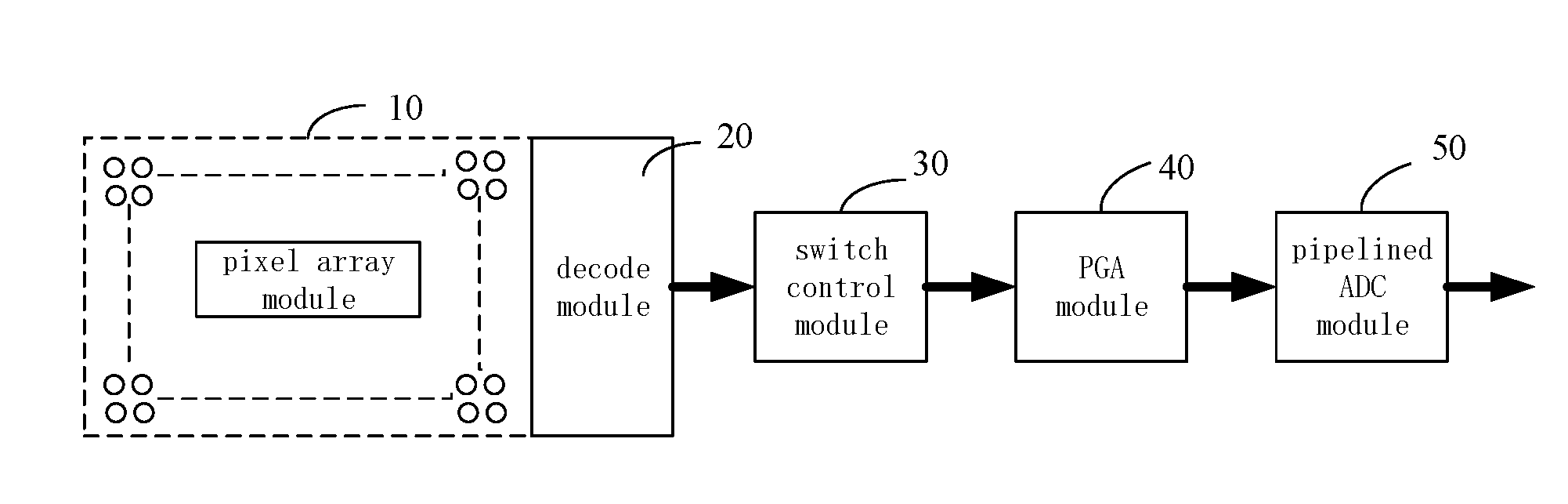
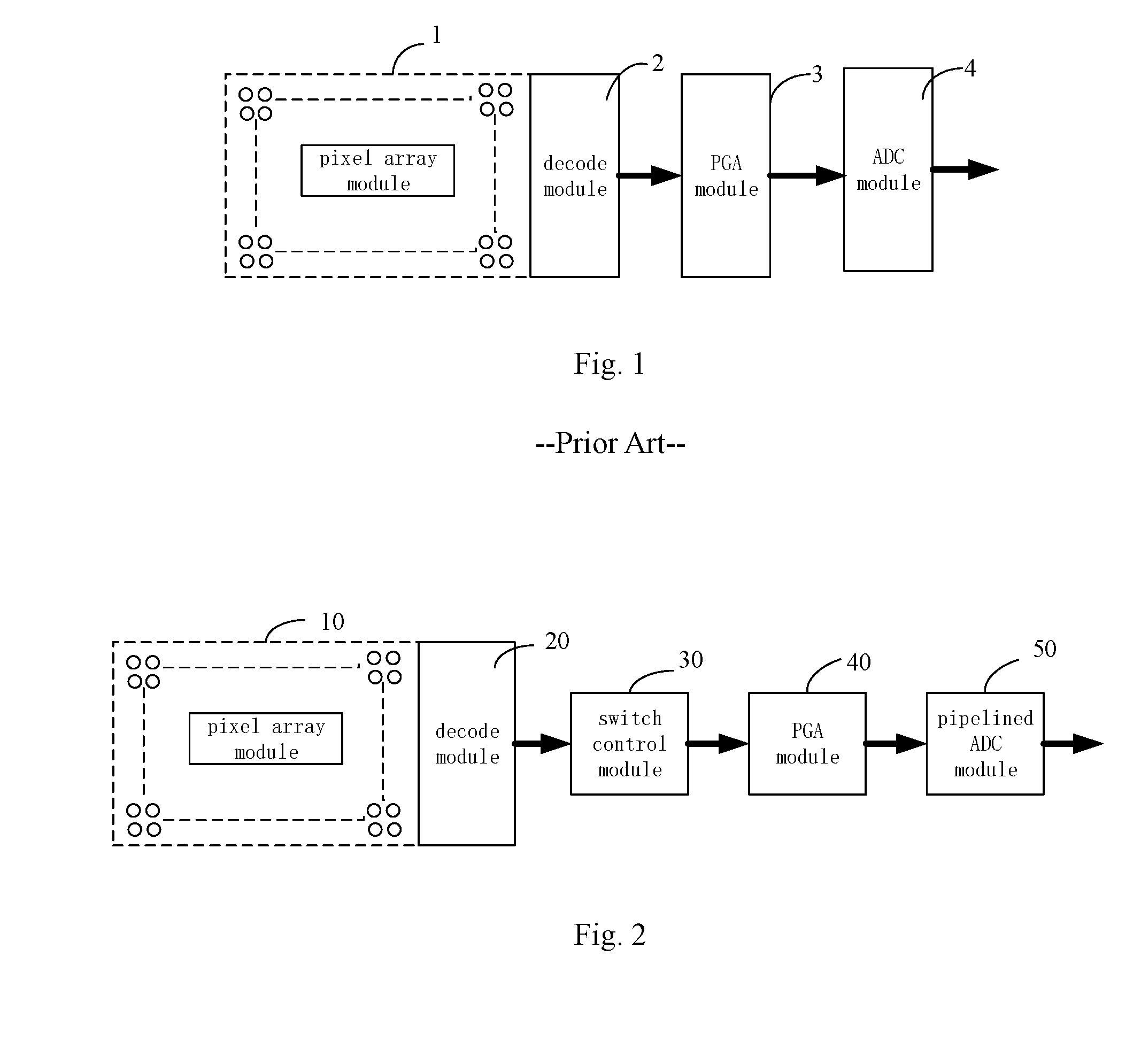
[0047]FIG. 2 is a block diagram of the image sensor of the present invention. As shown in FIG. 2, the image sensor comprises a pixel array module 10, a decode module 20, a switch control module 30, a PGA (programmable gain amplifier) module 40 and a pipelined ADC (analog-to-digital converter) module 50. The pixel array module 10 can be a pixel array formed by a plurality of pixel groups arranged in a matrix of multiple rows and multiple columns. Each pixel groups comprises multiple pixels, these pixels in one pixel group form at least one unit pixel. The multiple switch control modules 30 each corresponds to on...


PUM


Abstract

The present invention provides an image sensor comprising a pixel array module composed of pixel groups, multiple switch control modules, a PFA, a pipelined ADC and a decode module. Each pixel group comprises multiple unit pixels which form at least one unit pixel. Each switch control module corresponds to a row of the pixel array module and includes a first transmission circuit and a second transmission circuit. The PGA process the data outputted by the first and second transmission circuits and the pipelined ADC performs A/D conversion to the data outputted by the PGA. The decode module controls the first and second transmission circuits of each row to alternately read and transmit the unit pixel data, and controls all the first and second transmission circuits to successively output the data of the unit pixels readout thereby to the PGA.

Description

CROSS-REFERENCE TO RELATED APPLICATION[0001]This application claims the priority benefit of International Patent Application Serial No. PCT / CN2014 / 087,889, filed Sep. 30, 2014, which is related to and claims the priority benefit of China patent application serial No. 201410045272.3 filed Jan. 30, 2014. The entirety of each of the above-mentioned patent applications is hereby incorporated by reference herein and made a part of this specification.FIELD OF THE INVENTION[0002]The present invention relates to the field of image sensor and more particular to an image sensor and the data transmission method thereof.BACKGROUND OF THE INVENTION[0003]An image sensor, which can be either a CCD (charge coupled device) or a CMOS (complementary metal oxide silicon) image sensor, is an important component of a digital camera. Recently, the CMOS image sensor has been widely used due to its high pixel sensitivity, short exposure time and decreased pixel size. As one of the most important performance...

Claims


Application Information

Patent Timeline
Patent Type & Authority Applications(United States)
IPC IPC(8): H04N5/378H04N5/347H04N5/374H01L27/146
CPCH04N5/378H04N5/374H04N5/347H01L27/14641H04N25/46H04N25/59H04N25/778H04N25/75
Inventor LI, CHENWEN, JIANXINZHAO, YUHANG
Owner SHANGHAI INTEGRATED CIRCUIT RES & DEV CENT
Why Eureka
Try Eureka