Semiconductor device, manufacturing method of the same, or display device including the same
Active Publication Date: 2016-11-03
SEMICON ENERGY LAB CO LTD
View PDF0 Cites 13 Cited by
Summary
Abstract
Description
Claims
Application Information
AI Technical Summary
This helps you quickly interpret patents by identifying the three key elements:
Problems solved by technology
Method used
Benefits of technology
Benefits of technology
The present patent text provides a novel semiconductor device that includes an oxide semiconductor film, and a method for manufacturing it. This new device can be used in display devices and offers a simple manufacturing process at low cost.
Problems solved by technology
However, signaldelay or the like is increased by parasitic capacitance that exists between a gate electrode and source and drain electrodes of an inverted staggered transistor and accordingly image quality of a display device degrades, which has posed a problem, as an increase in screen size of a display device proceeds, or a display device is provided with a higher resolution image (for example, a high-resolution display device typified by 4 k×2 k pixels (3840 pixels in the horizontal direction and 2160 pixels in the perpendicular direction) or 8 k×4 k pixels (7680 pixels in the horizontal direction and 4320 pixels in the perpendicular direction)).
Furthermore, as another problem, the occupation area of an inverted staggered transistor is larger than that of a staggered transistor.
Method used
Image
Click on the blue label to locate the original text in one second.
Reading with bidirectional positioning of images and text.
Examples
embodiment 1
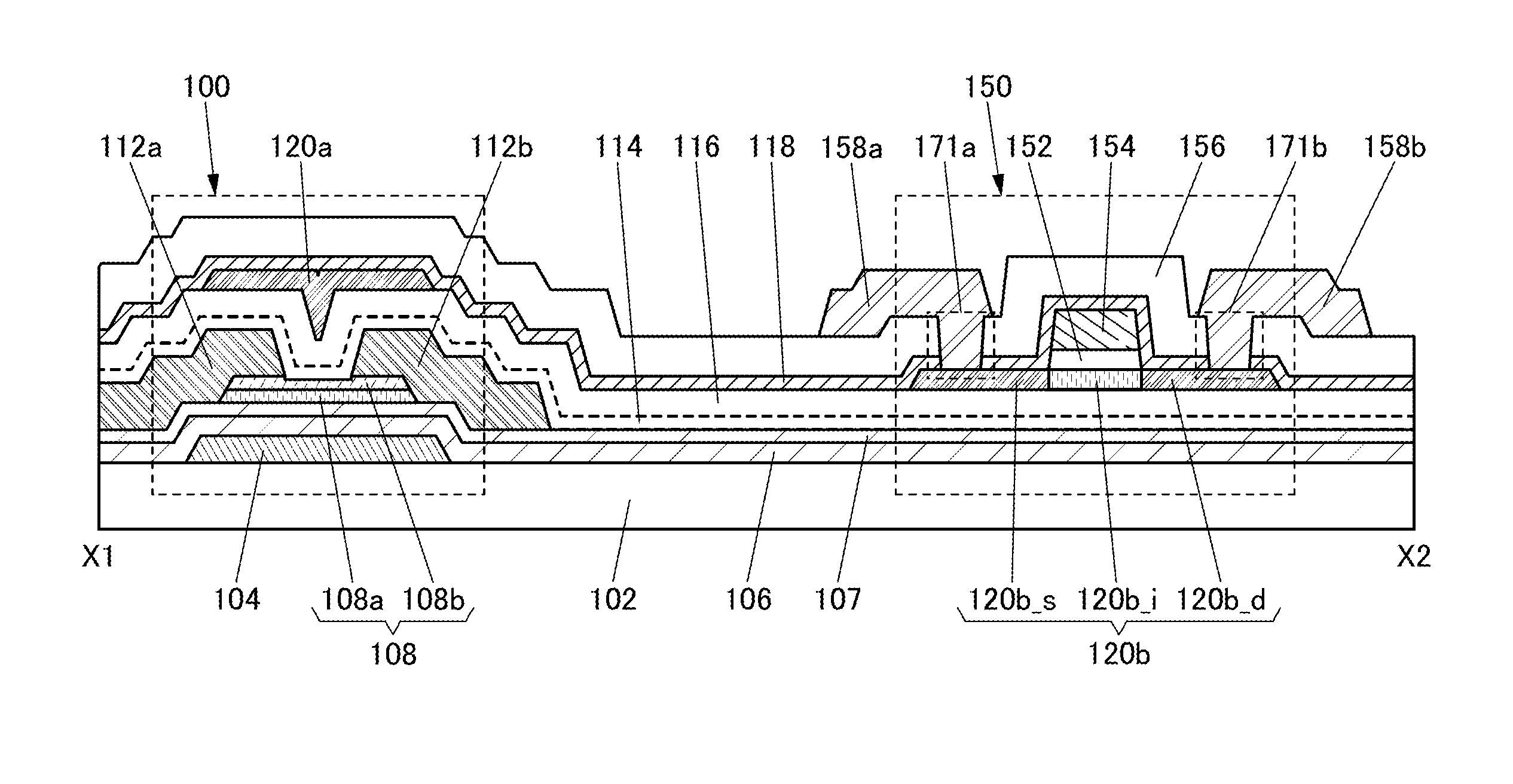
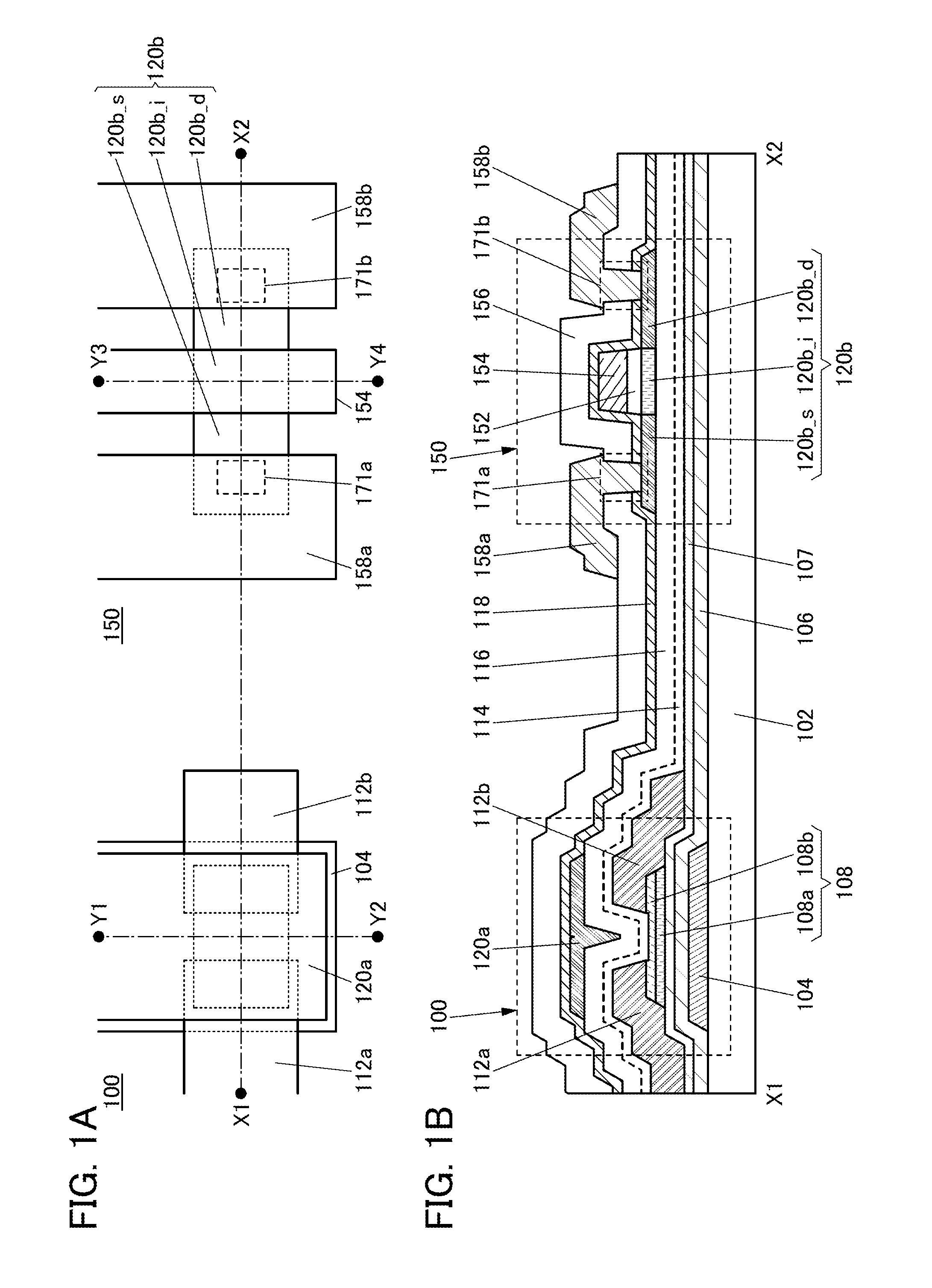
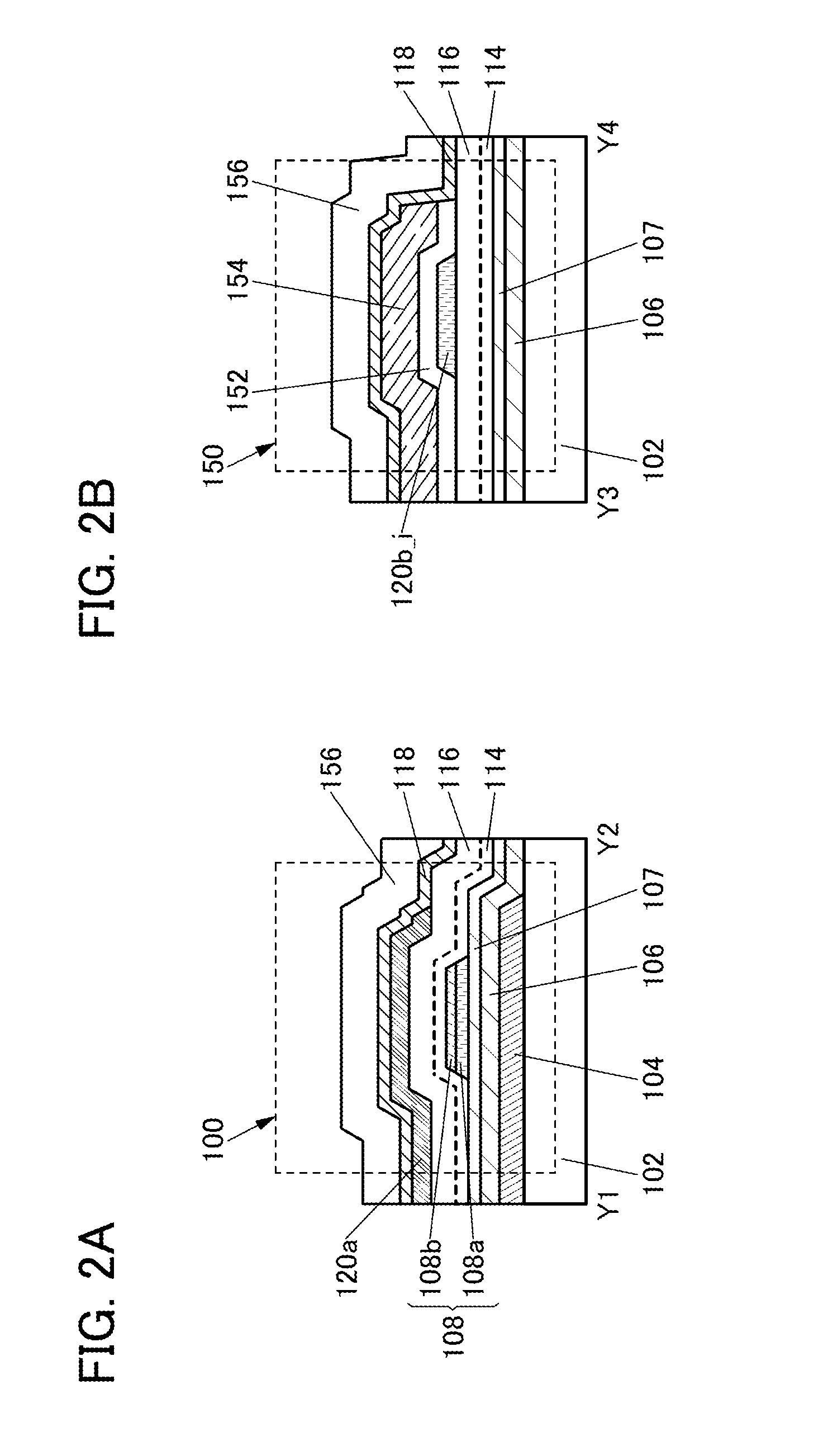
[0094]In this embodiment, a semiconductor device of one embodiment of the present invention and a method of manufacturing the semiconductor device are described with reference to FIGS. 1A and 1B, FIGS. 2A and 2B, FIGS. 3A and 3B, FIG. 4, FIGS. 5A and 5B, FIG. 6, FIGS. 7A and 7B, FIGS. 8A and 8B, FIGS. 9A and 9B, FIGS. 10A and 10B, FIGS. 11A and 11B, FIGS. 12A and 12B, FIGS. 13A and 13B, FIGS. 14A and 14B, FIGS. 15A and 15B, FIGS. 16A and 16B, FIGS. 17A and 17B, FIGS. 18A and 18B, FIGS. 19A and 19B, FIGS. 20A and 20B, FIGS. 21A and 21B, and FIG. 22.
[0095]FIG. 1A is a top view of a transistor 100 and a transistor 150 that are semiconductor devices of one embodiment of the present invention. FIG. 1B is a cross-sectional view taken along the dashed-dotted line X1-X2 in FIG. 1A. FIG. 2A is a cross-sectional view taken along the dashed-dotted line Y1-Y2 in FIG. 1A, and FIG. 2B is a cross-sectional view taken along the dashed-dotted line Y3-Y4 in FIG. 1A.
[0096]Note that in FIG. 1A, some co...
embodiment 2
[0316]In this embodiment, a structure of an oxide semiconductor and the like are described with reference to FIGS. 26A to 26E, FIGS. 27A to 27E, FIGS. 28A to 28D, FIGS. 29A and 29B, and FIG. 30.
[0317]An oxide semiconductor is classified into a single crystal oxide semiconductor and a non-single-crystal oxide semiconductor. Examples of a non-single-crystal oxide semiconductor include a c-axis aligned crystalline oxide semiconductor (CAAC-OS), a polycrystalline oxide semiconductor, a nanocrystalline oxide semiconductor (nc-OS), an amorphous-like oxide semiconductor (a-like OS), and an amorphous oxide semiconductor.
[0318]From another perspective, an oxide semiconductor is classified into an amorphous oxide semiconductor and a crystalline oxide semiconductor. Examples of a crystalline oxide semiconductor include a single crystal oxide semiconductor, a CAAC-OS, a polycrystalline oxide semiconductor, and an nc-OS.
[0319]An amorphous structure is generally thought to be isotropic and have n...
embodiment 3
[0358]In this embodiment, a display device including a semiconductor device of one embodiment of the present invention is described with reference to FIGS. 31A and 31B, FIGS. 32A and 32B, FIG. 33, FIG. 34, and FIG. 35. Note that in this embodiment, a structure in which a liquid crystal element is used as a display element of a display device (a liquid crystal display device) is specifically described.
[0359]A liquid crystal display device 880 in FIG. 31A includes a pixel portion 871, a gate driver 874, a source driver 876, m scan lines 877 which are arranged parallel or substantially parallel to each other and whose potentials are controlled by the gate driver 874, and n signal lines 879 which are arranged parallel or substantially parallel to each other and whose potentials are controlled by the source driver 876. Further, the pixel portion 871 includes a plurality of pixels 870 arranged in a matrix. Furthermore, common lines 875 arranged parallel or substantially parallel to each o...
PUM
Abstract
To provide a novel semiconductor device including an oxidesemiconductor film. The semiconductor device includes a first transistor and a second transistor. The first transistor includes a first gate electrode, a first insulating film over the first gate electrode, a first oxide semiconductor film over the first insulating film, a source electrode electrically connected to the first oxide semiconductor film, a drain electrode electrically connected to the first oxide semiconductor film, a second insulating film over the first oxide semiconductor film, a second oxide semiconductor film functioning as a second gate electrode, over the second insulating film, and a third insulating film over the second oxide semiconductor film. The second transistor includes a third oxide semiconductor film including a channel region, a source region, and a drain region over the second insulating film, a fourth insulating film over the channel region, a third gate electrode over the fourth insulating film, and the third insulating film over the source region and the drain region.
Description
BACKGROUND OF THE INVENTION[0001]1. Field of the Invention[0002]One embodiment of the present invention relates to a semiconductor device including an oxide semiconductor film. Another embodiment of the present invention relates to a display device including the semiconductor device. Another embodiment of the present invention relates to a manufacturing method of the semiconductor device including the oxide semiconductor film.[0003]Note that one embodiment of the present invention is not limited to the above technical field. The technical field of one embodiment of the invention disclosed in this specification and the like relates to an object, a method, or a manufacturing method. In addition, the present invention relates to a process, a machine, manufacture, or a composition of matter. In particular, one embodiment of the present invention relates to a semiconductor device, a display device, a light-emitting device, a power storage device, a storage device, a driving method thereo...
Claims
Application Information
Patent Timeline
Application Date:The date an application was filed.
Publication Date:The date a patent or application was officially published.
First Publication Date:The earliest publication date of a patent with the same application number.
Issue Date:Publication date of the patent grant document.
PCT Entry Date:The Entry date of PCT National Phase.
Estimated Expiry Date:The statutory expiry date of a patent right according to the Patent Law, and it is the longest term of protection that the patent right can achieve without the termination of the patent right due to other reasons(Term extension factor has been taken into account ).
Invalid Date:Actual expiry date is based on effective date or publication date of legal transaction data of invalid patent.

