Eureka AIR delivers breakthrough ideas for toughest innovation challenges, trusted by R&D personnel around the world.

Scan Driving Circuit and NOR Gate Logic Operation Circuit Thereof

Active Publication Date: 2016-11-24
TCL CHINA STAR OPTOELECTRONICS TECH CO LTD
View PDF3 Cites 0 Cited by
  • Summary
  • Abstract
  • Description
  • Claims
  • Application Information

AI Technical Summary

Benefits of technology

The disclosure describes a new scan driving circuit for a liquid crystal display that solves a design problem by using a combination of NTFT and invertor. This circuit replaces the original function of a PMOS element and realizes a characteristic similar to the original COMS NOR operation circuit, allowing for a larger scale digital integrated circuit to be integrated into the display. The technical effect of the disclosure is to improve the performance and functionality of the scan driving circuit for a liquid crystal display.

Problems solved by technology

Therefore, how to use a single element (PTFT or NTFT) to manufacture an inverter, a NAND or a NOR has become a serious problem.

Method used


Image

  • Scan Driving Circuit and NOR Gate Logic Operation Circuit Thereof
  • Scan Driving Circuit and NOR Gate Logic Operation Circuit Thereof
  • Scan Driving Circuit and NOR Gate Logic Operation Circuit Thereof

Examples


Embodiment Construction

[0031]The following description with reference to the accompanying drawings is provided to clearly and completely explain the exemplary embodiments of the disclosure. It is apparent that the following embodiments are merely some embodiments of the disclosure rather than all embodiments of the disclosure. According to the embodiments in the disclosure, all the other embodiments attainable by those skilled in the art without creative endeavor belong to the protection scope of the disclosure.

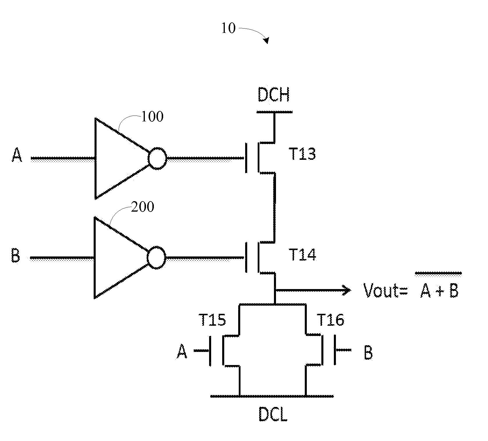
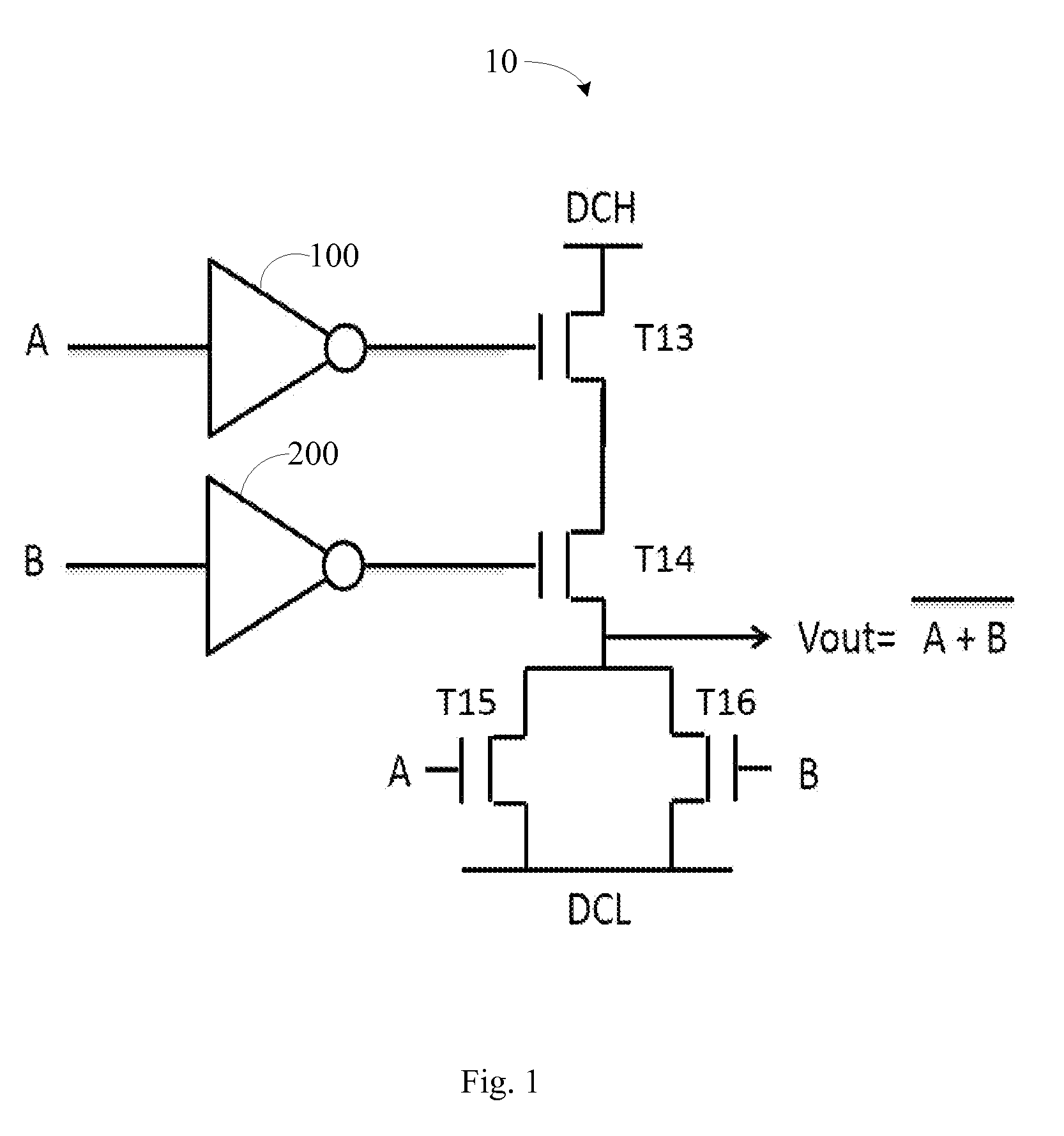
[0032]Refer to FIG. 1. FIG. 1 is a circuit diagram of the NOR gate logic operation circuit according to the embodiment of the disclosure. The NOR gate logic operation circuit 10 is applied to a logic operation circuit of a scan driving circuit for an oxide semiconductor thin film transistor.

[0033]The circuit 10 includes a first invertor 100 and a second invertor 200, wherein both of the first invertor 100 and the second invertor 200 are applied in a pull down holding circuit of a GOA circuit.

[0034]...


PUM


Abstract

The disclosure is related to a scan driving circuit for an oxide semiconductor thin film transistor and the NOR gate logic operation circuit thereof. The NOR gate logic operation circuit includes a first invertor and a second invertor applied in the pull down holding circuit of the GOA circuit, and a plurality of transistors. The combination of the NTFT and the invertor displaces the original function of the PMOS element to realize a characteristic similar to an original COMS NOR operation circuit, thereby solving a design problem of the logic operation circuit using a IGZO TFT single element, such that a larger scale digital integrated circuit is further suitably integrated into the liquid crystal display.

Description

BACKGROUND[0001]1. Technical Field[0002]The disclosure is related to liquid crystal display technology field, and more particular to a scan driving circuit for an oxide semiconductor thin film transistor and a NOR gate logic operation circuit thereof.[0003]2. Related Art[0004]For a large scale integrated circuit, three most basic elements in a logic operation circuit are an inverter, a NAND gate, or a NOR gate. Generally, the three elements are manufactured by using CMOS FET, i.e. the circuit includes two elements of PMOS and NMOS.[0005]In an oxide semiconductor element, IGZO has become the focus of attention for the next generation display, and the oxide semiconductor has better NTFT characteristic due to the special material structure. However, the thin film transistor (TFT) also has two elements of PTFT and NTFT, but only in LTPS process, a PTFT element with better performance is obtained. Therefore, how to use a single element (PTFT or NTFT) to manufacture an inverter, a NAND or...

Claims


Application Information

Patent Timeline
IPC IPC(8): G09G3/36H03K19/0944H01L27/12H03K19/20
CPCG09G3/3677H01L27/1225H03K19/0944H03K19/20G09G3/20G09G2300/0404G09G2310/0267G09G2310/0286G09G2310/0291
Inventor DAI, CHAO
Owner TCL CHINA STAR OPTOELECTRONICS TECH CO LTD
Why Eureka
Eureka Blog
Learn More