Multi-Layer Ceramic Capacitor and Method of Producing the Same

US20160351335A1Active Publication Date: 2016-12-01TAIYO YUDEN KK
4 Cites 37 Cited by

Patent Information

Authority / Receiving Office
US · United States
Current Assignee / Owner
Publication Date
2016-12-01

Smart Images

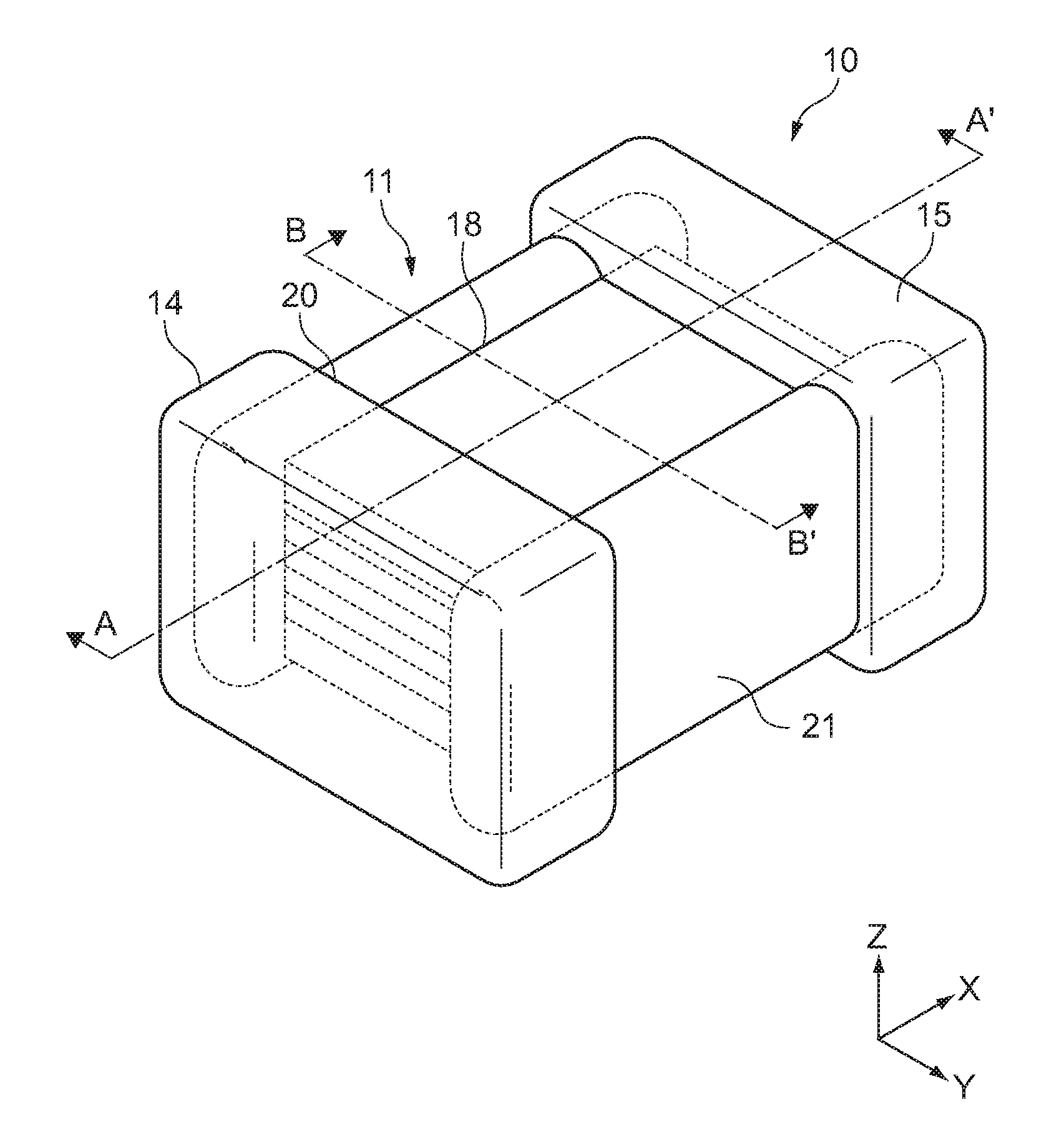
  • Figure 1
    Figure 1
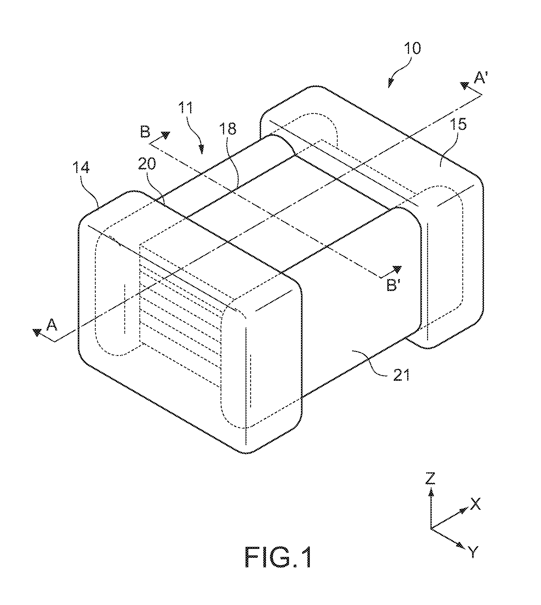
  • Figure 2
    Figure 2
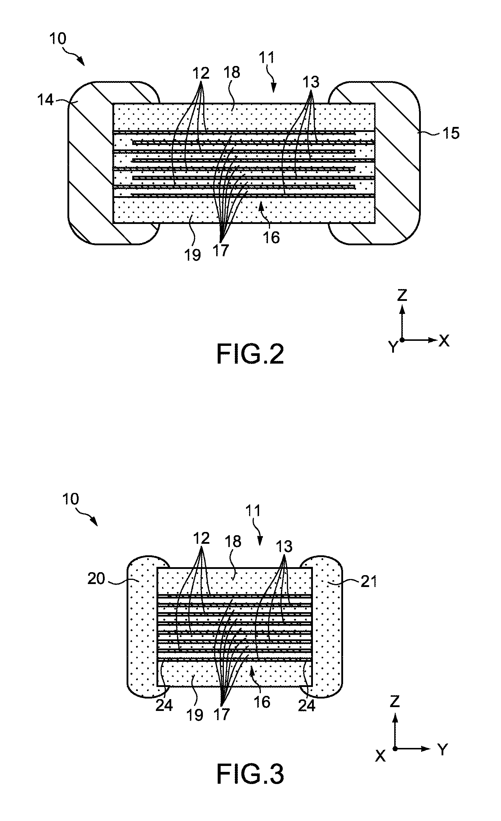
  • Figure 3
    Figure 3
Patent Text Reader

Abstract

A multi-layer ceramic capacitor according to an embodiment of the present invention includes a multi-layer, side margins and offset sections. The multi-layer includes internal electrodes and dielectric layers alternately laminated. The side margins are configured of a dielectric and disposed to cover side faces of the multi-layer. The offset sections are made with amorphous areas or gap areas. The offset sections are formed between the internal electrodes and the side margins such that ends at side faces of the internal electrodes are offset from the side faces to an inward direction of the multi-layer.
Need to check novelty before this filing date? Find Prior Art

Description

CROSS REFERENCE TO RELATED APPLICATIONS

[0001] This application claims priority under 35 U.S.C. §119 to Japanese Patent Application Nos. 2015-109660, filed May 29, 2015; and 2016-053325, filed Mar. 17, 2016, which are hereby incorporated by reference in their entirety.BACKGROUND

[0002] The present invention relates to a multi-layer ceramic capacitor that is applicable to miniaturization and capacity enlargement.BRIEF SUMMARY

[0003] In recent years, along with miniaturization and capacity enlargement of electronic devices, the miniaturization and the capacity enlargement of multi-layer ceramic capacitors used in the electronic devices are increasingly demanding. In order to increase the capacity while suppressing the size of the multi-layer ceramic capacitors, it is effective to enlarge intersection areas of internal electrodes of the multi-layer ceramic capacitor (areas where the internal electrodes faced are overlapped) as great as possible.

[0004] According to a technology developed for e...

Examples

examples

[0109]The embodiment of the present invent on will be described. The multi-layer ceramic capacitor 10 (hereinafter referred to as an “experimental chip”) having the following configuration was produced by the above-described production method.

[0110]Configuration of experimental chip

[0111]Chip size (W×D×H): 1.0 mm×0.5 mm×0.5 mm (including external electrodes)

[0112]Thickness of dielectric layer: 0.7 μm

[0113]Number of dielectric layers: 315

[0114]Thickness of internal electrode layer: 0.7 μm

[0115]Number of internal electrode layers: 315

[0116]Thickness of cover layer: 35 μm

[0117]Thickness of side margin: 30

[0118]Thickness of external electrode (including plating): 30 μm

[0119]Thickness of end margin: 50 μm

[0120]The thickness of the end margin is a minimum value of a distance between an edge of the internal electrode layer at an external electrode side where no internal electrode is drawn and the external electrode (for example, a distance between the internal electrodes 12 and the externa...