Light emitting element, light-emitting device, display device, electronic device, and lighting device
a technology of light-emitting devices and light-emitting elements, which is applied in the direction of luminescent compositions, organic chemistry, chemistry apparatus and processes, etc., can solve the problems of difficult optimization of excited levels, no guideline for selecting substances, and serious limitations on molecular design. , to achieve the effect of high emission efficiency, high efficiency and high emission efficiency
- Summary
- Abstract
- Description
- Claims
- Application Information
AI Technical Summary
Benefits of technology
Problems solved by technology
Method used
Image
Examples
embodiment 1
[0074]As a method for converting a triplet excited state into light emission, there are a method utilizing phosphorescence, which is direct emission from a triplet excited state, and a method utilizing delayed fluorescence, which is light emitted from a singlet excited state after a triplet excited state is turned into a singlet excited state via reverse intersystem crossing.
[0075]A structure of a light-emitting element that uses a phosphorescent material and emits light with extremely high efficiency has been reported, which proves advantages of the utilization of a triplet excited state for light emission. However, central metals of phosphorescent materials are mostly rare metals, and there are concerns about cost and supply in mass production.
[0076]Some degree of success in a light-emitting element using a delayed fluorescence material has been achieved in recent years. However, a substance emitting delayed fluorescence with relatively high efficiency has an extremely rare state ...
embodiment 2
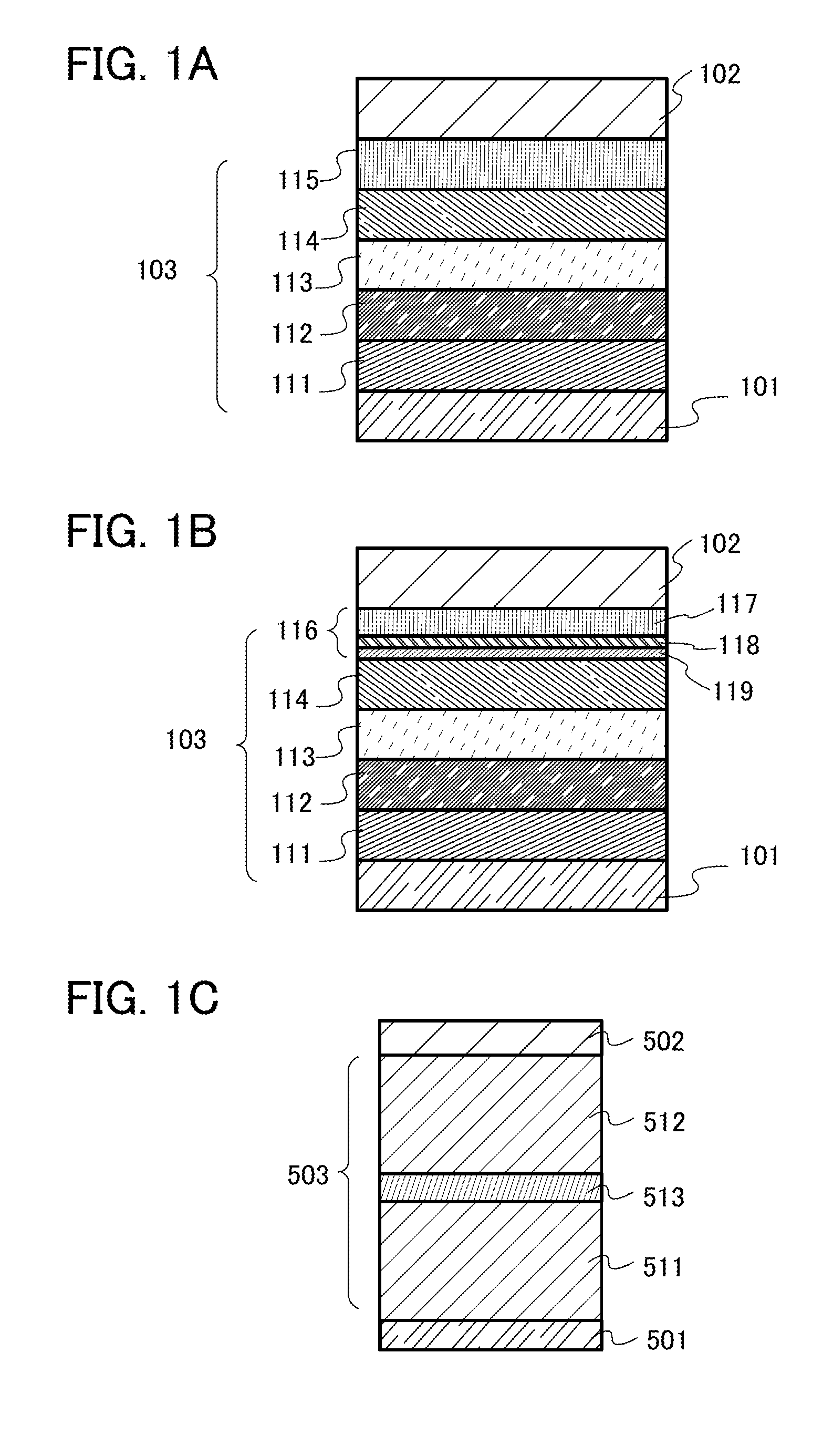
[0136]In this embodiment, a detailed example of the structure of the light-emitting element described in Embodiment 1 will be described below with reference to FIGS. 1A and 1B.
[0137]In FIG. 1A, the light-emitting element includes a first electrode 101, a second electrode 102, and a layer 103 containing organic compounds and provided between the first electrode 101 and the second electrode 102. Note that in this embodiment, the following description is made on the assumption that the first electrode 101 functions as an anode and that the second electrode 102 functions as a cathode.
[0138]To function as an anode, the first electrode 101 is preferably formed using any of metals, alloys, conductive compounds having a high work function (specifically, a work function of 4.0 eV or more), mixtures thereof, and the like. Specific examples include indium oxide-tin oxide (ITO: indium tin oxide), indium oxide-tin oxide containing silicon or silicon oxide, indium oxide-zinc oxide, and indium oxi...
example 1
[0248]In this example, light-emitting elements 1 to 4 which are the light-emitting elements of embodiments of the present invention described in Embodiment 1 of the present invention will be described. Structural formulae of organic compounds used for light-emitting elements 1 to 4 are shown below.
(Method for Fabricating Light-Emitting Element 1)
[0249]First, silicon or indium tin oxide containing silicon oxide (ITSO) was formed on a glass substrate by a sputtering method to form the first electrode 101. It is to be noted that the film thickness of the first electrode was set to be 110 nm and that the area of the electrode was set to be 2 mm×2 mm.
[0250]Next, in pretreatment for forming the light-emitting element over the substrate, a surface of the substrate was washed with water and baked at 200° C. for one hour, and then UV ozone treatment was performed for 370 seconds.
[0251]After that, the substrate was transferred into a vacuum evaporation apparatus where the pressure had been re...
PUM
 Abstract
Description
Claims
Application Information


