Input front-end circuit for switching power supply control integrated circuit and switching power supply controller having the same

Active Publication Date: 2016-12-15
FUJI ELECTRIC CO LTD
View PDF2 Cites 0 Cited by
  • Summary
  • Abstract
  • Description
  • Claims
  • Application Information

AI Technical Summary

Benefits of technology

The patent describes a method to prevent malfunctions and noise in a control circuit by using a signal voltage from the input front-end circuit. This ensures that the operating points and control amounts for each function are consistent with the input voltage, and also helps to distinguish voltage within the control IC from zero voltage when the lowest input voltage is received. Overall, this improves the accuracy of signal processing in the control circuit.

Problems solved by technology

When the input voltage is high, the divided voltage is 1V to less than 2V and is sufficient for a range of internal circuit operations, but when a low input voltage is detected, for example when 45 Vdc is detected, the signal is extremely low at 0.18V and close to the lower limit of the input range for the receiving-side internal circuit of the control IC, thereby mixing with noise within the control IC and making it difficult to distinguish between the signal and the noise, which causes the control IC to malfunction and / or falsely detect.
For the same reason, it also becomes difficult to define, with high accuracy, the circuit characteristics using the control IC specifications.
However, using such a configuration may be inconvenient due to problems such as errors from the AMP 103 being applied to the input part of function block B.
In other words, it is inconvenient that a function group for executing a plurality of functions based on a single input does not act together based on information on a plurality of inputs.
This inconvenience is allowed as long as the control mode switching points are only slightly unaligned, but in a worst-case scenario, the control mode switching needs an excessive amount of responses from the switching control, potentially causing hunting.
For power-factor correction control ICs in particular, it is necessary to detect the timing at which the circuit current crosses zero using the IS terminal shown in FIG. 1 of Patent Document 3, for example; thus, it is difficult to handle miniscule voltages, which may lead to malfunctions.

Method used


Image

  • Input front-end circuit for switching power supply control integrated circuit and switching power supply controller having the same
  • Input front-end circuit for switching power supply control integrated circuit and switching power supply controller having the same
  • Input front-end circuit for switching power supply control integrated circuit and switching power supply controller having the same

Examples


embodiment 1

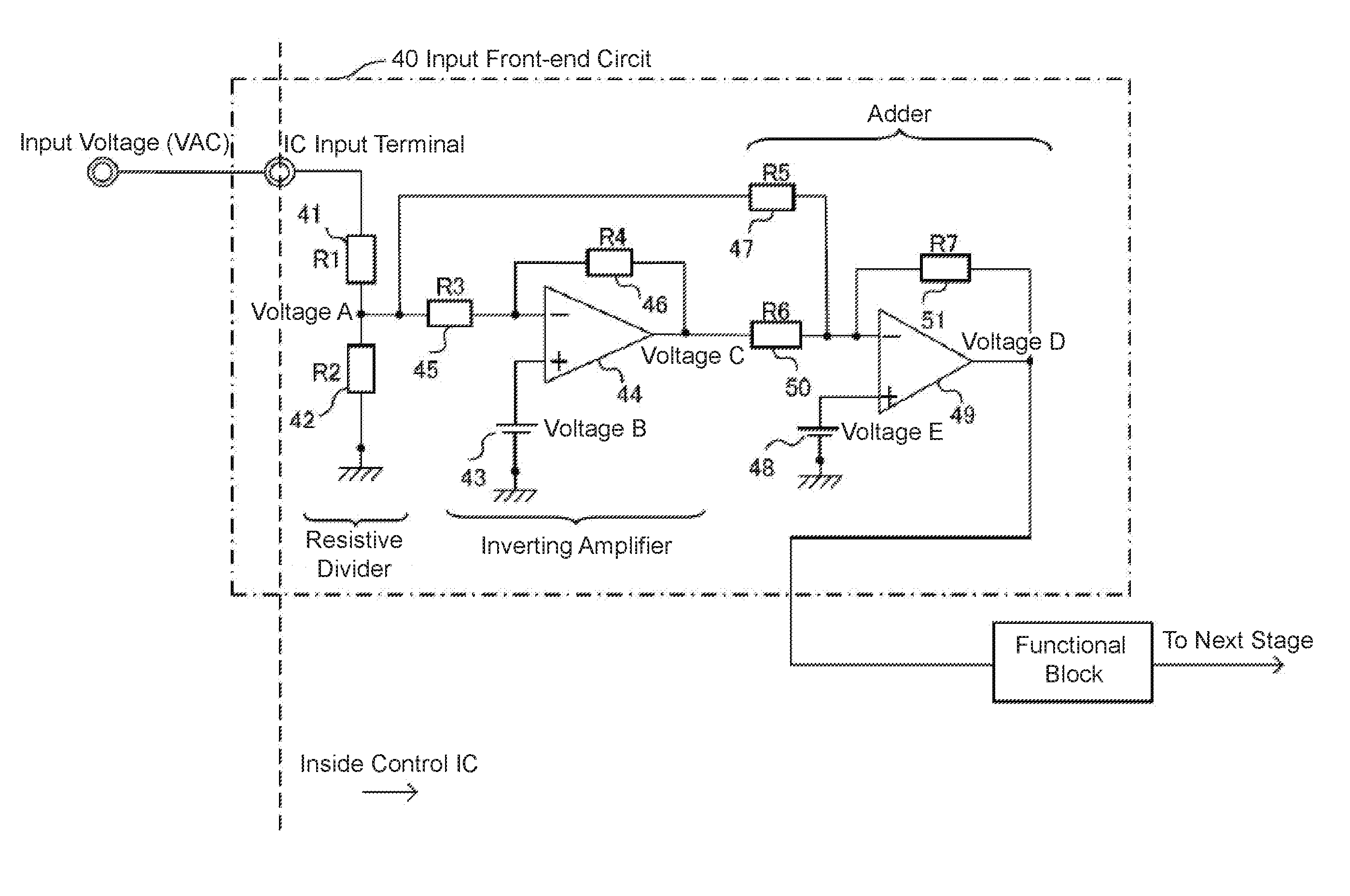
[0042]FIG. 1 shows the configuration of an input front-end circuit for a switching power supply control IC according to Embodiment 1 of the present invention. The operations of the input front-end circuit 40 according to Embodiment 1 of the present invention are described using FIG. 1.

[0043]The input front-end circuit 40 shown in FIG. 1 divides input voltage from a wide input voltage range (voltage VAC from a rectified alternating-current commercial power supply, for example) using a resistive divider unit, sends the input voltage into a control IC unit, and then carries out signal processing.

[0044]Specifically, (1) a voltage A is created by dividing the input voltage (VAC, for example) using resistors R1 (41) a R2 (42).

[0045](2) A voltage C is created by inverting and amplifying the voltage A using an inverting amplifier (inverting amplifier 1; first inverting amplifier) with a reference point, voltage B (43), which is configured to be lower than the internal voltage of the control...

embodiment 2

[0054]FIG. 3 shows the configuration of an input front-end circuit for a switching power supply control IC according to Embodiment 2 of the present invention. The configuration of an input front-end circuit 60 according to Embodiment 2 of the present invention shown in FIG. 3 is the same as the configuration of the input front-end circuit 40 according to Embodiment 1 of the present invention shown in FIG. 1, except that the feedback resistor R5 of the adder has been removed and that the adder has been substituted with a single input inverting amplifier 2.

[0055]In the configuration shown in FIG. 3, the inverting amplifier 2 is provided instead of the adder shown in FIG. 1, and the voltage C, which is the output of the inverting amplifier 1, is level shifted using the inverting amplifier 2 to obtain the voltage D. Note that the inverting amplifier 2 is composed of an inverting amplifier circuit. The inverting amplifier circuit is composed of an operational amplifier (68), a reference ...

embodiment 3

[0058]FIG. 4 shows the configuration of an input front-end circuit for a switching power supply control IC according to Embodiment 3 of the present invention. For Embodiment 3, the voltage-dividing resistors R1 (41), R2 (42) from Embodiment 1 shown in FIG. 1 are removed, and the resistor R3 (45) is directly connected to the input voltage going through the input terminal. This configuration corresponds to when the input voltage (VAC, for example) is divided using an external element outside of the control IC, for example. Note that the inverting amplifier is composed of an inverting amplifier circuit. The inverting amplifier circuit is composed of an operational amplifier (82), a reference voltage (81), and resistors R3 (83), R4 (84). The adder is composed of an inverting amplifier circuit. The inverting amplifier circuit is composed of an operational amplifier (87), a reference voltage (86), and resistors R5 (85), R6 (88), R7 (89).

[0059]The operations of an input front-end circuit 8...


PUM


Abstract

An inverting amplifier creates a voltage C using a reference voltage (voltage B) as a reference point. An adder composed of two input inverting amplifier circuits ultimately creates a voltage D by carrying out weighted addition of the voltage A and the voltage C. By using the voltage D created by an input front-end circuit, the internal functions of the control IC can prevent the operating points and control amounts for each function from being different relative to the input voltage and make it possible to distinguish voltage within the control IC from zero voltage when the lowest input voltage is received.

Description

BACKGROUND OF THE INVENTIONTechnical Field[0001]The present invention relates to input front-end circuits used when external signals are sent to a switching power supply control IC.Background Art[0002]Input pre-circuits convert voltage that an integrated circuit (IC) receives an external source such that the voltage is in a range that is appropriate for processing by a circuit within the IC itself. FIG. 5 shows the first of two example configurations of a conventional input front-end circuit for a switching power supply control IC. In addition, FIG. 6 shows an example configuration of a general switching power supply device configured to include a switching power supply control IC 8.[0003]In FIGS. 5 and 6, respectively, the reference character 1 represents an AC input (input voltage VAC), 2 represents a transformer for forming an input filter, 3 represents a capacitor for forming the input filter, 4 represents a diode bridge for rectifying the AC input, 5 represents a capacitor for ...

Claims


Application Information

Patent Timeline
IPC IPC(8): G06G7/14H02M3/335H02M1/08
CPCG06G7/14H02M2001/0006H02M3/33507H02M1/08H02M3/335H02M1/0006
Inventor HIASA, NOBUYUKI
Owner FUJI ELECTRIC CO LTD
Why Eureka
Try Eureka