Solid state wideband fourier transform infrared spectrometer

a fourier transform and infrared spectrometer technology, applied in the field of infrared spectrometry, can solve the problems of intrinsically susceptible to misalignment and/or damage, high mechanical precision and cost required to realize such improved implementations, and achieve high flux and peak power levels, long interaction lengths

Active Publication Date: 2016-12-29
BAE SYST INFORMATION & ELECTRONICS SYST INTERGRATION INC
View PDF41 Cites 7 Cited by
  • Summary
  • Abstract
  • Description
  • Claims
  • Application Information

AI Technical Summary

Benefits of technology

[0006]The use of silicon for the waveguide material significantly reduces the cost of manufacturing the interferometer, and in various embodiments a germanium detector is grown on the wafer, thus simplifying the packaging and reducing cost still further. Other embodiments include heterogeneous integration of an indium gallium arsenide (“InGaAs”) detector diode.
[0009]In exemplary embodiments of the present invention, the spectrometer is used in a standoff configuration, wherein the sample to be measured is located at some distance from the spectrometer. Other embodiments take advantage of the small size of the invention to eliminate the 1 / R2 loss in sensitivity that is typical of standoff sampling systems by placing the sample in a sample space provided within the spectrometer, so that the interferometer is very close to the sample being measured. The spectrometer sensitivity can be greatly increased for some of these embodiments through the use of an onboard active light source, such as a glow bar. In embodiments, the sample space can be exposed to the surrounding air to allow detection and analysis of any chemical that may be present in the ambient atmosphere.
[0010]Materials such as LiNbO4 (“LN”), Zinc Germanium Phosphide (“ZGP”), and many other materials, some of which are well established and others of which are still under development, possess both transparency and high optical polarizability, and can be used in various embodiments in place of OpGaAs as an up-converting and / or down-converting medium.
[0011]The recent perfection of parallel technology in both non-linear poled materials such as OpGaAs and Si-photonics platforms is a key enabler of the present invention. In some embodiments, waveguide devices constructed of these new converter materials allow very small, commercially available cyclooctatetraene (“COT”) CW laser diodes to generate the baseband spectral inputs (“BBSI”) from approximately 1.2 to 1.6 microns that are required by these Si / SiO2 filter devices. The CW outputs of these COT laser diodes, typically with output powers as low as 1-10 milliwatts, experience long interaction lengths in the guided modes of the waveguides, which efficiently converts, for example, the long-wave, information-rich spectral telltale signatures in the signal to the BBSI wavelength range. The relative spectral locations, widths, and intensities are thereby mapped into the converted wavelengths.
[0012]This waveguide conversion approach overcomes the natural tendency of tightly focused optical drive or pump beams to diverge, and thereby maintains the beam intensities that are required for conversion. This enables the use of simple CW pumps, which provide electrical and optical simplicity, because it eliminates the need for short-pulse pump lasers, which typically require complex and inefficient electro-optical components and accompanying high flux and peak power levels that are known to place stress on other material in the beam path.

Problems solved by technology

However, a high degree of mechanical precision and cost has been required to realize such improved implementations.
Also, even for the more rugged configurations, the mechanical nature of the Michelson interferometer design renders it intrinsically susceptible to misalignment and / or damage.

Method used


Image

  • Solid state wideband fourier transform infrared spectrometer
  • Solid state wideband fourier transform infrared spectrometer
  • Solid state wideband fourier transform infrared spectrometer

Examples


Embodiment Construction

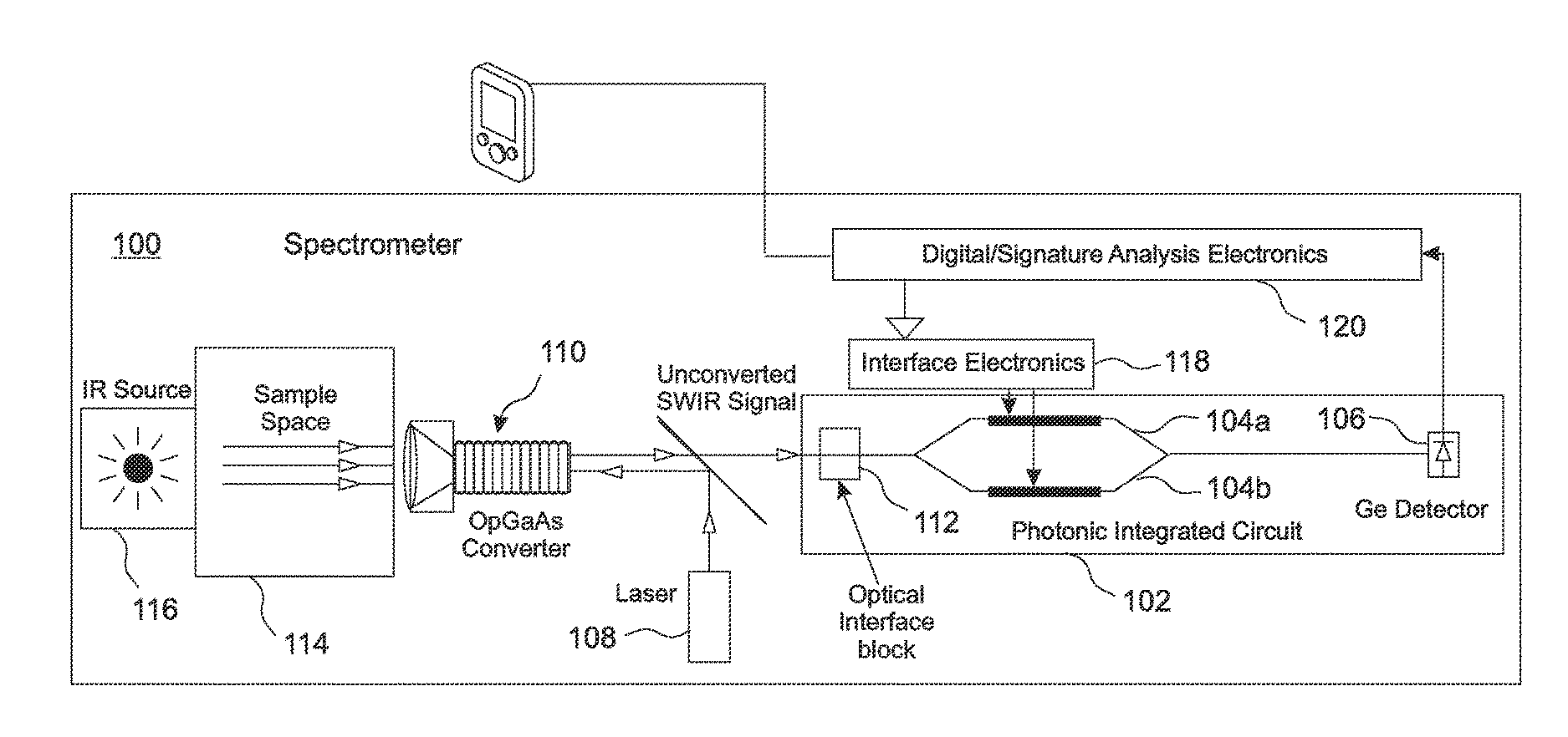
[0037]With reference to FIG. 1, a novel FTIR spectrometer 100 that is less expensive to manufacture and smaller in size than conventional FTIR spectrometers based on the Michelson design includes a Mach-Zehnder interferometer 102 that is realized in silicon and includes no moving parts. The optical path lengths of the two waveguide arms 104a, 104b of the interferometer 102 are varied under control of interface electronics 118 by changing the index of refraction of the waveguide material. In some embodiments, this is done by heating the waveguides, while in other embodiments this is accomplished by changing the carrier concentration of the Si in the waveguides. This latter approach is achieved by configuring each arm 104 as either a “p-n” or “p-i-n” diode and by changing the electrical bias conditions of the diodes. In embodiments, the optical path lengths of both of the arms 104 are driven in opposite directions; that is, one arm 104a is made optically longer, while the other arm 10...


PUM

PropertyMeasurementUnit
absorption edgeaaaaaaaaaa
wavelength rangeaaaaaaaaaa

Abstract

A compact, low cost FTIR spectrometer with no moving parts includes an interferometer having optical paths through silicon waveguides. The optical path lengths are varied by changing the temperature and / or carrier density of at least one of the waveguides. In embodiments, the interferometer is a Mach-Zehnder interferometer. Embodiments vary both optical path lengths in opposite directions. In embodiments, a germanium or InGaAs IR detector is grown on the same wafer as the waveguides. Embodiments include a laser pump, such as a COT CW diode laser, and wavelength mixer, such as an OPGaAs or OPGaP converter, for up and / or down converting measured IR wavelengths into a range compatible with the waveguide and detector materials. The wavelength mixer can be a waveguide. Embodiments include a sample compartment and an IR source such as a glowbar. In embodiments, the sample compartment can be exposed to ambient atmosphere for analysis of gases contained therein.

Description

RELATED APPLICATIONS[0001]This application claims the benefit of U.S. Provisional Application No. 62 / 079,185, filed Nov. 13, 2014, which is herein incorporated by reference in its entirety for all purposes.FIELD OF THE INVENTION[0002]The invention relates to infrared spectrometry, and more particularly, to Fourier transform infrared spectrometers.BACKGROUND OF THE INVENTION[0003]Fourier transform infrared (“FTIR”) spectrometers have been in use for decades for routine chemical analysis. The FTIR concept is built on the use of an interferometer that can scan over many null and maximum points. Typically, FTIR spectrometers have used mechanical interferometers that are based on the Michelson design. These mechanical FTIR systems have demonstrated excellent performance over a wide wavelength range. In addition, some implementations of the Michelson approach have been made smaller and more rugged over time through careful design. However, a high degree of mechanical precision and cost ha...

Claims


Application Information

Patent Timeline
Patent Type & Authority Applications(United States)
IPC IPC(8): G01J3/453G01B9/02G01N21/3504G01J3/02G01J3/10
CPCG01J3/453G01J3/0205G01J3/108G01N21/3504G01N2021/3595G01N2201/0612G01N2201/061G01N2201/08G01B9/02015G01J3/4531G01J3/4532
Inventor MOFFITT, PAUL R.KETTERIDGE, PETER A.
Owner BAE SYST INFORMATION & ELECTRONICS SYST INTERGRATION INC
Why Eureka
Try Eureka