Ips in-cell touch display panel and manufacturing method thereof

a touch display panel and in-cell technology, applied in the field of display technology, can solve the problems of limited product thinning, poor sensitivity of in-cell touch control, high cost, etc., and achieve the effects of low manufacturing cost, high manufacturing efficiency, and simple manufacturing operation

Inactive Publication Date: 2016-12-29
TCL CHINA STAR OPTOELECTRONICS TECH CO LTD
View PDF6 Cites 11 Cited by
  • Summary
  • Abstract
  • Description
  • Claims
  • Application Information

AI Technical Summary

Benefits of technology

[0008]An object of the present invention is to provide an in-plane switching (IPS) in-cell touch display panel, which has a simple manufacturing operation, a low manufacturing cost, and a high manufacturing efficiency.

Problems solved by technology

However, due to factors, such as higher technical difficulty and being susceptible to signal interference, the sensitivity of the in-cell touch control is generally poor.
Advantages of the external mounting type include high sensitivity and fast response speed, but there are also disadvantages including high cost and limitation on product thinning.

Method used


Image

  • Ips in-cell touch display panel and manufacturing method thereof
  • Ips in-cell touch display panel and manufacturing method thereof
  • Ips in-cell touch display panel and manufacturing method thereof

Examples


Embodiment Construction

[0047]To further expound the technical solution adopted in the present invention and the advantages thereof, a detailed description is given to a preferred embodiment of the present invention and the attached drawings.

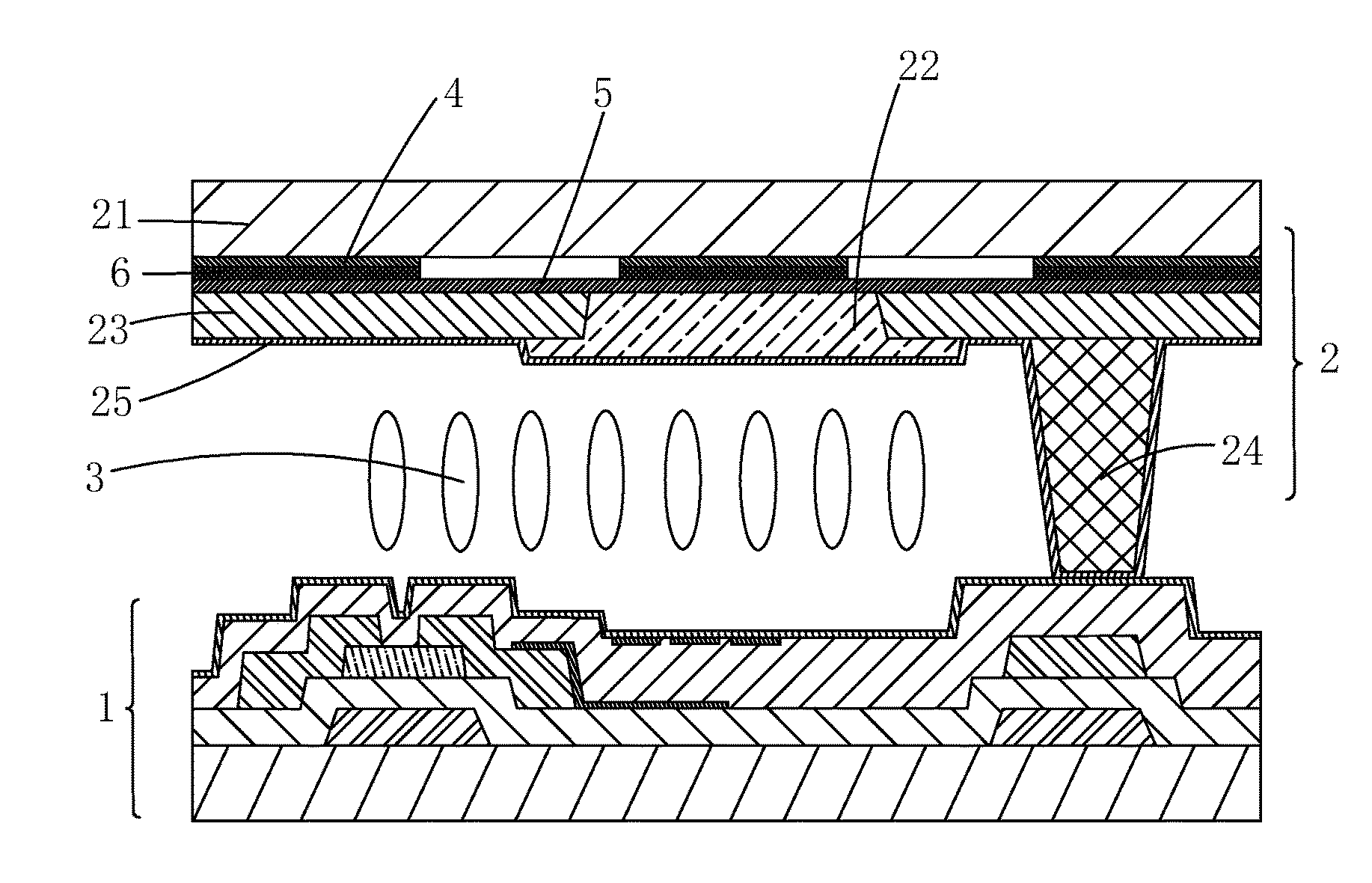
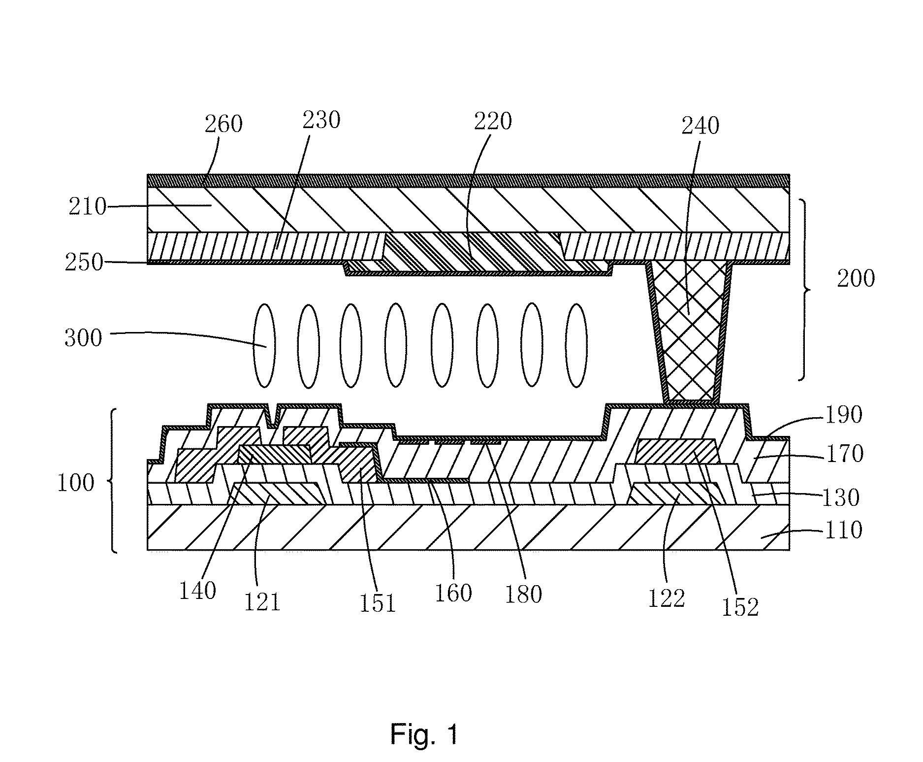
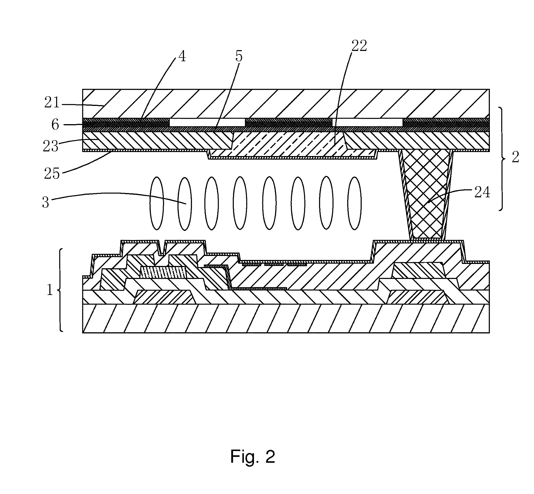
[0048]Referring collectively to FIGS. 2-4, firstly, the present invention provides an in-plane switching (IPS) in-cell touch display panel, which comprises a thin-film transistor (TFT) array substrate 1, a color filter (CF) substrate 2 opposite to the TFT array substrate 1, a liquid crystal layer 3 interposed between the TFT array substrate 1 and the CF substrate 2, a plurality of touch transmission electrodes 4 parallel to each other and arranged on a surface of the CF substrate 2 that is adjacent to the liquid crystal layer 3, and a plurality of touch receiving electrodes 5 parallel to each other and perpendicularly intersecting the touch transmission electrodes 4 in space. Insulation is achieved by a plurality of insulating photoresist blocks 6 arranged at locations...


PUM

PropertyMeasurementUnit
temperatureaaaaaaaaaa
thicknessaaaaaaaaaa
transparentaaaaaaaaaa

Abstract

The present invention provides an IPS in-cell touch display panel and a manufacturing method thereof. The IPS in-cell touch display panel includes insulating photoresist blocks (6) arranged at intersections between touch transmission electrodes (4) and touch receiving electrodes (5) for insulation. The method applies a grey-tone mask and etching operation to form touch transmission electrodes (4) and preserves portions of an organic photoresist that correspond to intersections in perpendicularity between the touch transmission electrodes (4) and touch receiving electrodes (5) to form insulating photoresist blocks (6) to allow insulation to be achieved between the touch transmission electrodes (4) and the touch receiving electrodes (5) with the insulating photoresist blocks (6) so that coating and masking and etching operations specifically for making an insulation layer can be eliminated to thereby simplify the manufacturing operation of a touch display panel, reduce the manufacturing cost, and increase the manufacturing efficiency; and in addition, the touch transmission electrodes (4) and the touch receiving electrodes (5) provide an effect of electromagnetic shielding to capacitance of the liquid crystal layer so that there is no need to specifically form a protection electrode.

Description

BACKGROUND OF THE INVENTION[0001]1. Field of the Invention[0002]The present invention relates to the field of display technology, and in particular to an in-plane switching (IPS) in-cell touch display panel and a manufacturing method thereof.[0003]2. The Related Arts[0004]With the rapid process of the display technology, touch display panels have been widely accepted and used by people. For example, intelligent phones and tablet computers both involve the use of touch display pane. The touch display panel is formed by applying the embedding touch technology to combine a touch panel and a liquid crystal display panel with each other as a unit with the functionality of the touch panel embedded in the liquid crystal display panel to make the liquid crystal display panel to simultaneously possess the functions of displaying and touch control / input.[0005]The liquid crystal display panels are generally made up of a color filter (CF) substrate, a thin-film transistor (TFT) array substrate,...

Claims


Application Information

Patent Timeline
Patent Type & Authority Applications(United States)
IPC IPC(8): G02F1/1333G02F1/1343G02F1/1339G02F1/1368G02F1/1337G06F3/041G02F1/1335
CPCG02F1/13338G06F3/0412G02F1/134363G02F1/133516G02F1/133512G02F1/1368G02F2001/133519G02F1/13439G02F1/1337G02F1/13394G06F2203/04103G06F2203/04107G02F1/134309G02F1/133345G06F2203/04111G06F3/0443G06F3/0446
Inventor XU, XIANGYANG
Owner TCL CHINA STAR OPTOELECTRONICS TECH CO LTD
Why Eureka
Try Eureka