Method of using a sacrifical gate structure to make a metal gate finfet transistor

a technology of finfet transistor and sacrifical gate structure, which is applied in the direction of semiconductor devices, basic electric elements, electrical equipment, etc., can solve the problems of increasing the strain of incorporating germanium atoms using existing methods, mechanical instability of the lattice structure of germanium-rich films, and affecting the mechanical stability of the lattice structure, etc., to achieve the effect of improving electron mobility

Active Publication Date: 2017-01-05
BELL SEMICON LLC
View PDF5 Cites 25 Cited by
  • Summary
  • Abstract
  • Description
  • Claims
  • Application Information

AI Technical Summary

Benefits of technology

[0008]Strain and mobility effects in the channel of a FinFET can be tuned by controlling the size and the elemental composition of the fins. It is advantageous for SiGe films to contain a high concentration of germanium, e.g., in the range of at least 25%-40%, to provide enhanced electron mobility compared with lower concentration SiGe films. Carrier mobility in the channel region determines overall transistor performance. Consequently, it is desirable to increase to a level as high as possible the percent concentration of germanium atoms in the fins of a SiGe FinFET.

Problems solved by technology

While a strained silicon lattice is beneficial, creating strain by incorporating germanium atoms using existing methods tends to damage the crystal lattice.
As a result, the lattice structures of germanium-rich films tend to be mechanically unstable, especially if they contain a high number of structural defects such as faults, or dislocations.
Furthermore, such a mechanically unstable fin may be structurally limited with regard to its aspect ratio, or height:width ratio.
Such a limitation is undesirable because one advantage of a FinFET is that the fin, being a vertical structure, has a small footprint.

Method used


Image

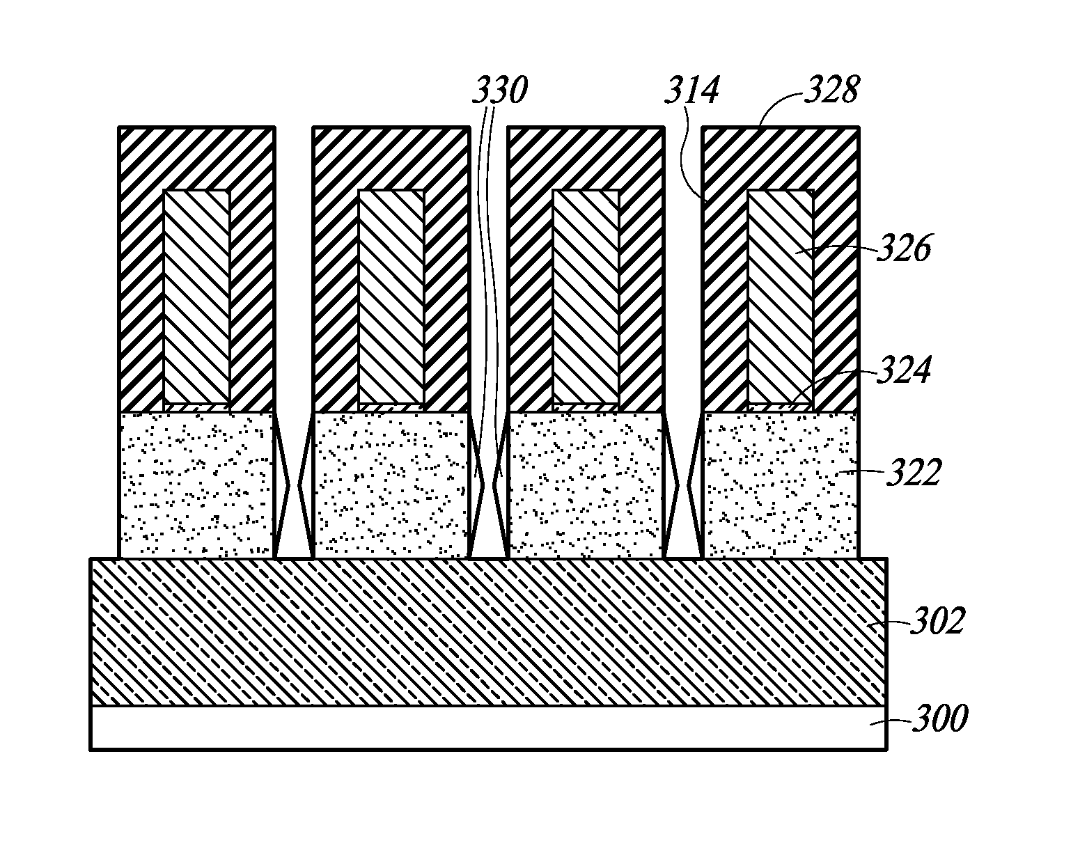
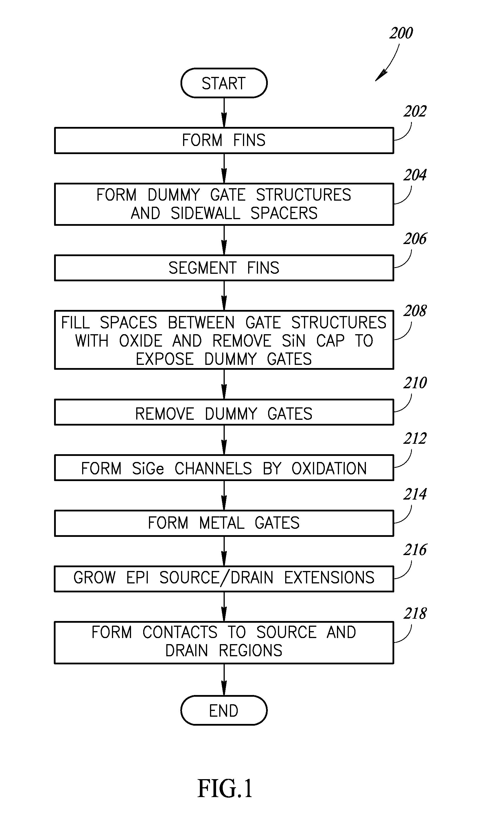
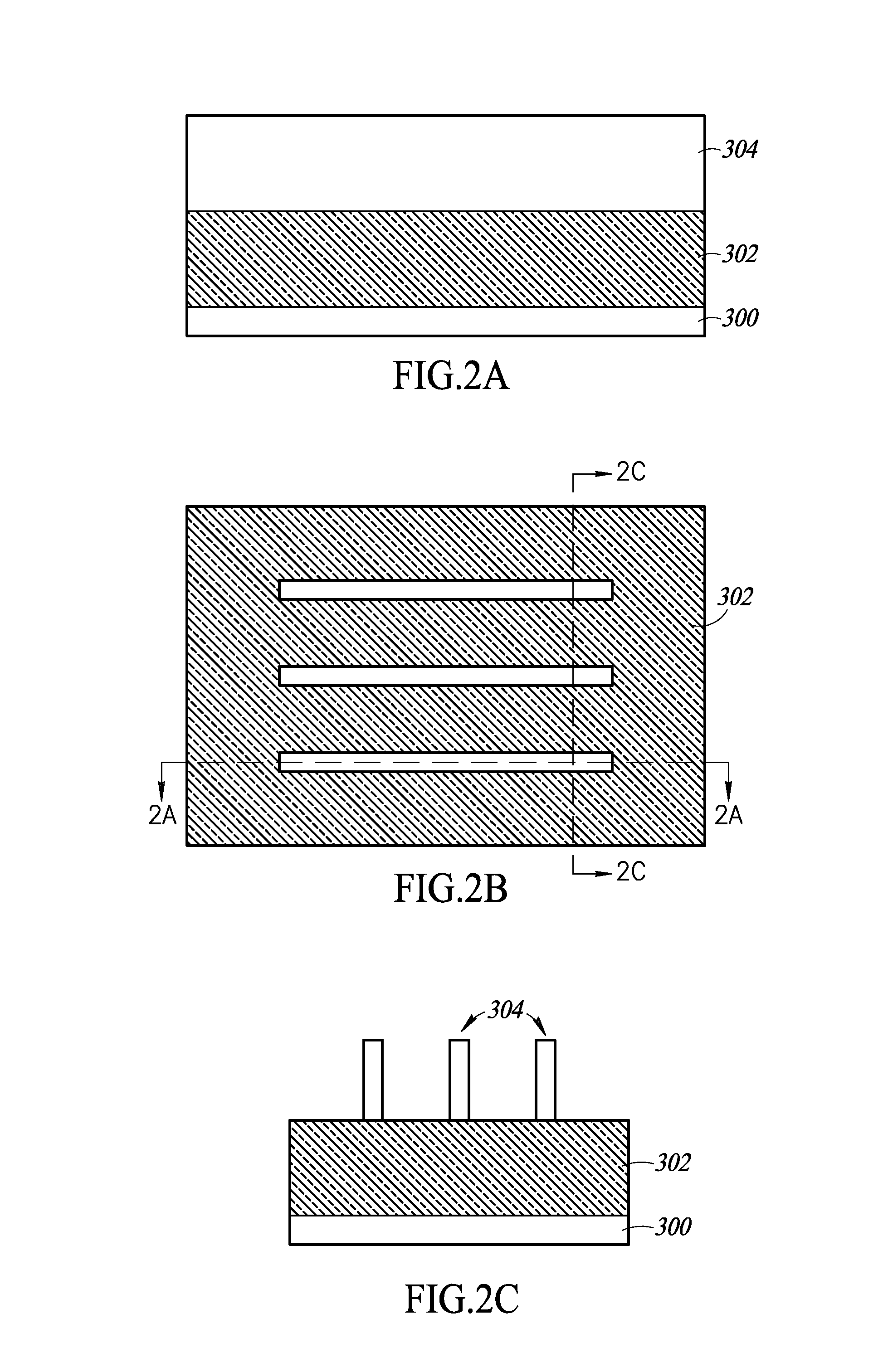
  • Method of using a sacrifical gate structure to make a metal gate finfet transistor
  • Method of using a sacrifical gate structure to make a metal gate finfet transistor
  • Method of using a sacrifical gate structure to make a metal gate finfet transistor

Examples


Embodiment Construction

[0021]In the following description, certain specific details are set forth in order to provide a thorough understanding of various aspects of the disclosed subject matter. However, the disclosed subject matter may be practiced without these specific details. In some instances, well-known structures and methods of semiconductor processing comprising embodiments of the subject matter disclosed herein have not been described in detail to avoid obscuring the descriptions of other aspects of the present disclosure.

[0022]Unless the context requires otherwise, throughout the specification and claims that follow, the word “comprise” and variations thereof, such as “comprises” and “comprising” are to be construed in an open, inclusive sense, that is, as “including, but not limited to.”

[0023]Reference throughout the specification to “one embodiment” or “an embodiment” means that a particular feature, structure, or characteristic described in connection with the embodiment is included in at le...


PUM


Abstract

A self-aligned SiGe FinFET device features a relaxed channel region having a high germanium concentration. Instead of first introducing germanium into the channel and then attempting to relax the resulting strained film, a relaxed channel is formed initially to accept the germanium. In this way, a presence of germanium can be established without straining or damaging the lattice. Gate structures are patterned relative to intrinsic silicon fins, to ensure that the gates are properly aligned, prior to introducing germanium into the fin lattice structure. After aligning the gate structures, the silicon fins are segmented to elastically relax the silicon lattice. Then, germanium is introduced into the relaxed silicon lattice, to produce a SiGe channel that is substantially stress-free and also defect-free. Using the method described, concentration of germanium achieved in a structurally stable film can be increased to a level greater than 85%.

Description

BACKGROUND[0001]1. Technical Field[0002]The present disclosure generally relates to techniques for fabricating an array of high performance FinFET devices.[0003]2. Description of the Related Art[0004]Advanced integrated circuits often feature strained channel transistors, silicon-on-insulator (SOI) substrates, FinFET structures, or combinations thereof, in order to continue scaling transistor gate lengths below 20 nm. Such technologies allow the channel length of the transistor to shrink while minimizing detrimental consequences such as current leakage and other short channel effects.[0005]A FinFET is an electronic switching device in which a conventional planar semiconducting channel is replaced by a semiconducting fin that extends outward from the substrate surface. In such a device, the gate, which controls current flow in the fin, wraps around three sides of the fin so as to influence current flow from three surfaces instead of one. The improved control achieved with a FinFET de...

Claims


Application Information

Patent Timeline
Patent Type & Authority Applications(United States)
IPC IPC(8): H01L29/10H01L29/161H01L29/66H01L29/06H01L29/417H01L29/78
Inventor LOUBET, NICOLASMORIN, PIERRE
Owner BELL SEMICON LLC
Why Eureka
Try Eureka