Silicon Controlled Rectifier

a rectifier and silicon technology, applied in the direction of semiconductor devices, electrical apparatus, transistors, etc., can solve the problems of device latching, scr shut down, and voltage across the scr needs to be reduced below the “hold voltage”

Active Publication Date: 2017-01-12
NXP BV
View PDF1 Cites 3 Cited by
  • Summary
  • Abstract
  • Description
  • Claims
  • Application Information

AI Technical Summary

Benefits of technology

[0027]The arrangement of the first and second MOSFETs and the trigger circuit may provide for effective triggering of the silicon controlled rectifier while allowing the biasing of the second region noted ab

Problems solved by technology

However, their main drawback is that, once activated, the voltage across the SCR needs to be decreased below its “hold voltage” to make the SCR shut down.
For short-base SCR's this hold voltage may lie in the range of 2-3 V. If such an SCR is implemented in a product that operates in the 3-5 V range, the device is prone to latch-up, which generally leads to device failure.
A disadvantage of a device of this kind is that

Method used


Image

  • Silicon Controlled Rectifier
  • Silicon Controlled Rectifier
  • Silicon Controlled Rectifier

Examples


Embodiment Construction

[0041]Embodiments of the present disclosure are described in the following with reference to the accompanying drawings.

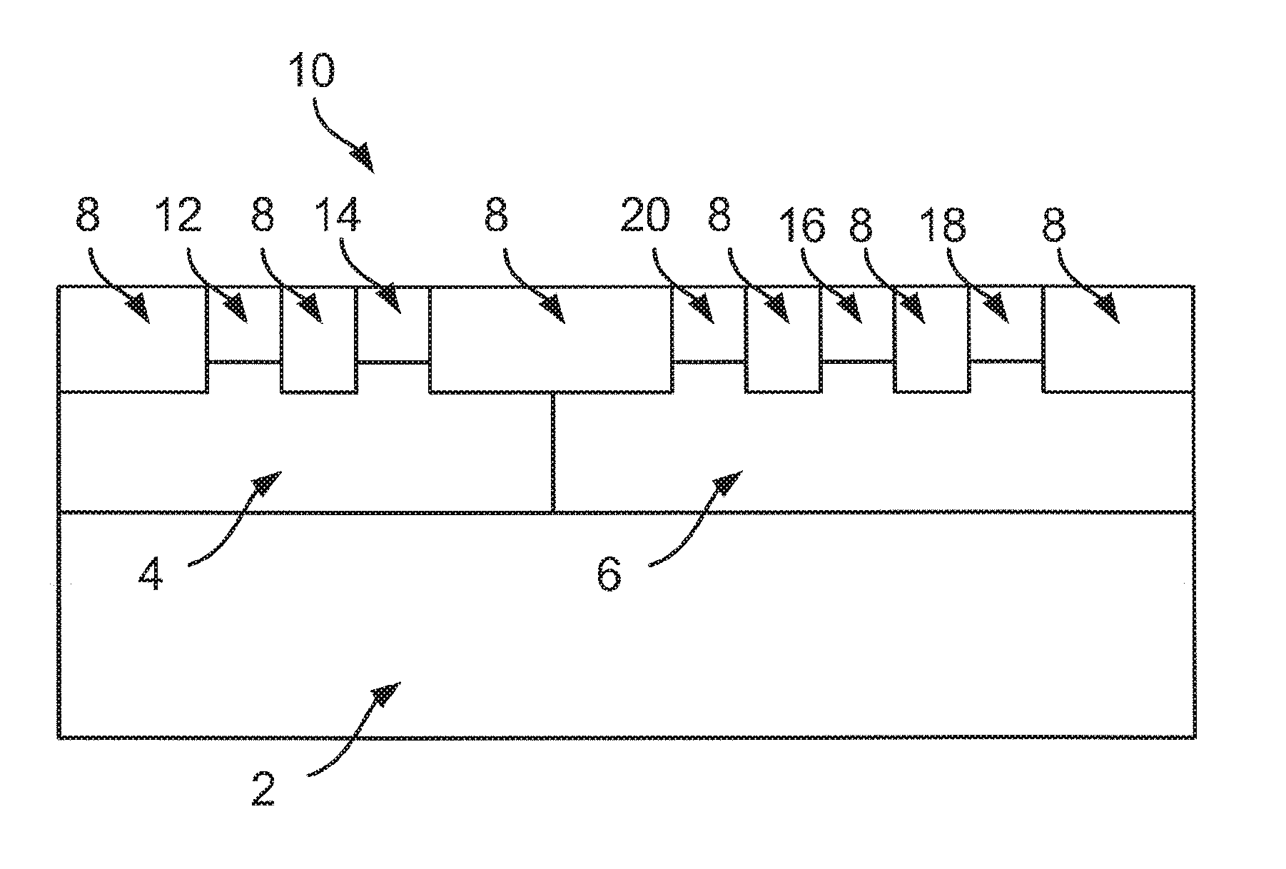
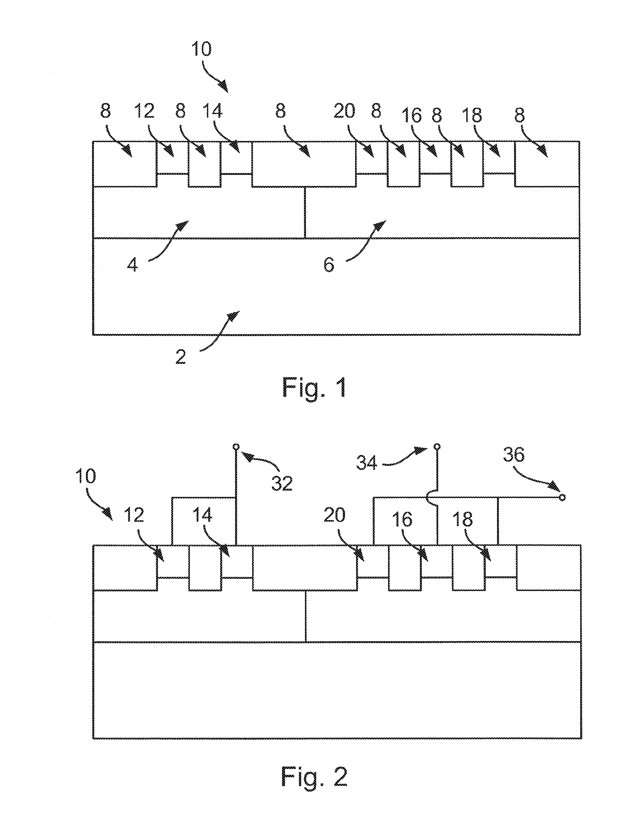
[0042]FIG. 1 shows a silicon controlled rectifier 10 in accordance with an embodiment of the present disclosure. The silicon controlled rectifier 10 may be provided in a semiconductor substrate 8. The substrate may, for instance, be a silicon substrate 8. The substrate may be doped to have a first conductivity type, which may be either p-type or n-type.

[0043]The silicon controlled rectifier 10 includes a first region 4 and a second region 6 located in the substrate 8. The second region 6 is located adjacent the first region 4. Each region 4, 6 may comprise a doped semiconductor material such as doped silicon. The first region 4 is doped to have a first conductivity type and the second region 6 is doped to have a second conductivity type (where the first and second conductivity types are different conductivity types). In the following examples, the first conductivity...


PUM


Abstract

A silicon controlled rectifier, an electrostatic discharge (ESD) protection circuit including the silicon controlled rectifier and an integrated circuit including the silicon controlled rectifier or ESD protection circuit. The silicon controlled rectifier includes a first region having a first conductivity type and a second region having a second conductivity type located adjacent the first region in a semiconductor substrate. A junction is formed at a boundary between the first region and the second region. Contact regions of the first conductivity type and the second conductivity type located in each of the first region and the second region. A further contact region of the second conductivity type is located in the second region, in between the contact region of the first conductivity type and the junction. The further contact region and the contact region of the second conductivity type in the second region are connected together for biasing the second region.

Description

FIELD OF THE INVENTION[0001]This invention relates to a silicon controlled rectifier, to an electrostatic discharge (ESD) protection circuit including the silicon controlled rectifier and to an integrated circuit including the silicon controlled rectifier or ESD protection circuit.BACKGROUND OF THE INVENTION[0002]Silicon Controlled Rectifiers (SCRs) are popular as electrostatic discharge (ESD) protection devices because of their capacity for handling large ESD currents while needing only a small amount of silicon area. However, their main drawback is that, once activated, the voltage across the SCR needs to be decreased below its “hold voltage” to make the SCR shut down. For short-base SCR's this hold voltage may lie in the range of 2-3 V. If such an SCR is implemented in a product that operates in the 3-5 V range, the device is prone to latch-up, which generally leads to device failure.[0003]A long-base SCR is an SCR engineered to have its holding voltage above the intended operati...

Claims


Application Information

Patent Timeline
IPC IPC(8): H01L27/02
CPCH01L27/0262H01L27/0292H01L27/0285H01L29/7436
Inventor DE RAAD, GIJS JANQUAX, GUIDO WOUTER WILLEM
Owner NXP BV
Why Eureka
Try Eureka