Anisotropic conductive film and method for manufacturing the same

a technology of anisotropic conductive film and conductive film, which is applied in the direction of removing conductive materials by irradiation, semiconductor/solid-state device details, instruments, etc., can solve the problems of reducing the width and interval of wirings, the inability to stably align circuit members on the substrate to be adhered thereto using the acf, and the decrease of the plane area of a non-display area of display devices

Active Publication Date: 2017-01-12
SAMSUNG DISPLAY CO LTD
View PDF4 Cites 15 Cited by
  • Summary
  • Abstract
  • Description
  • Claims
  • Application Information

AI Technical Summary

Problems solved by technology

Recently, display devices have been developed to have high definition, which may result in a planar area of a non-display area of the display devices decreasing, and the width and the interval of wirings decreasing.
Accordingly, there is a difficulty in stably aligning the circuit member on a substrate to be adhered thereto using the ACF.

Method used


Image

  • Anisotropic conductive film and method for manufacturing the same
  • Anisotropic conductive film and method for manufacturing the same
  • Anisotropic conductive film and method for manufacturing the same

Examples


Embodiment Construction

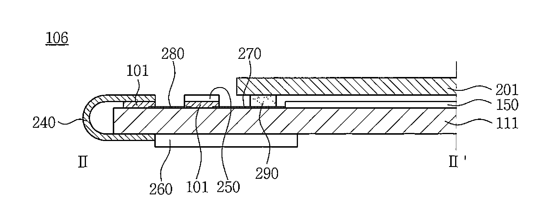
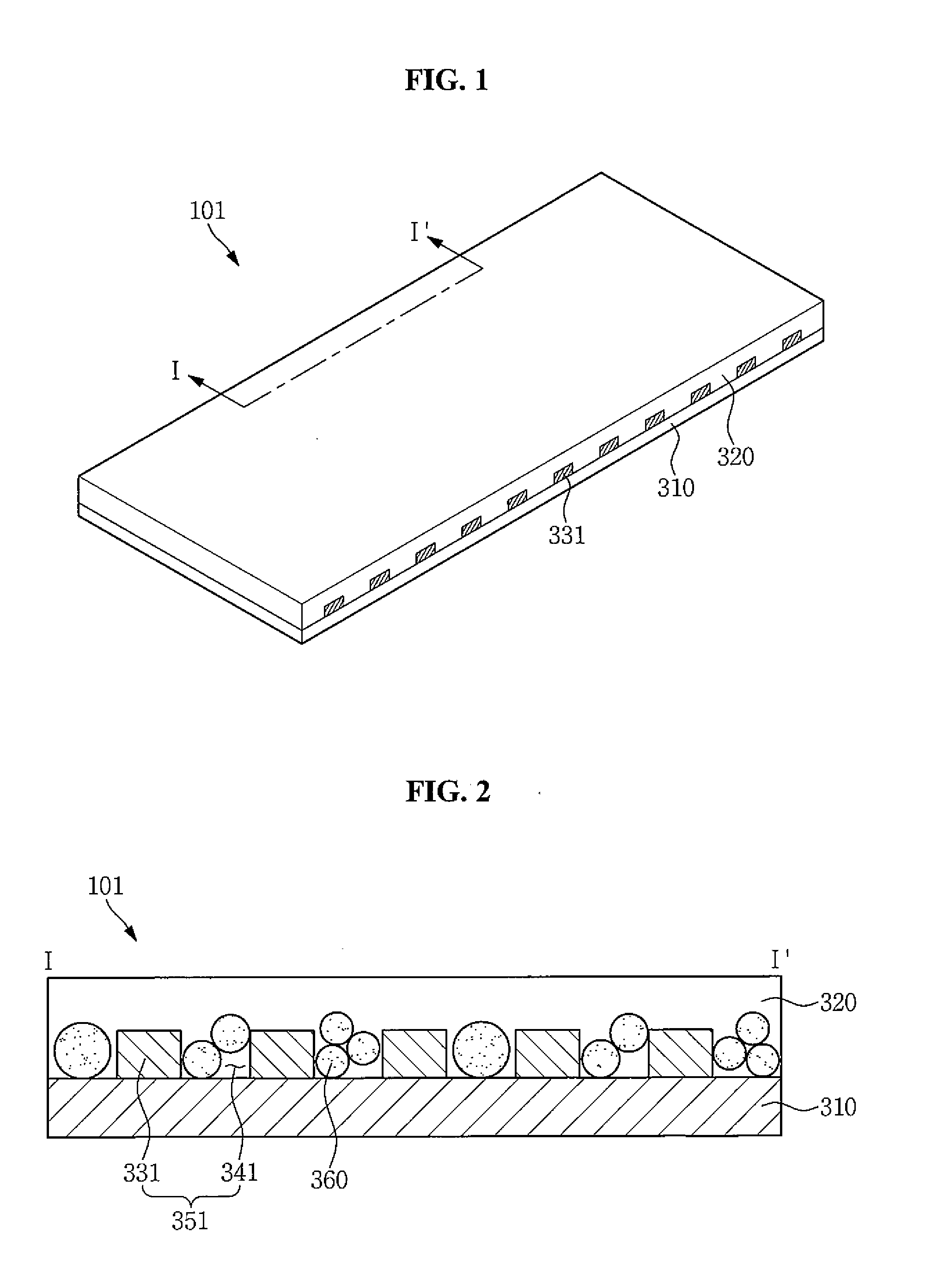
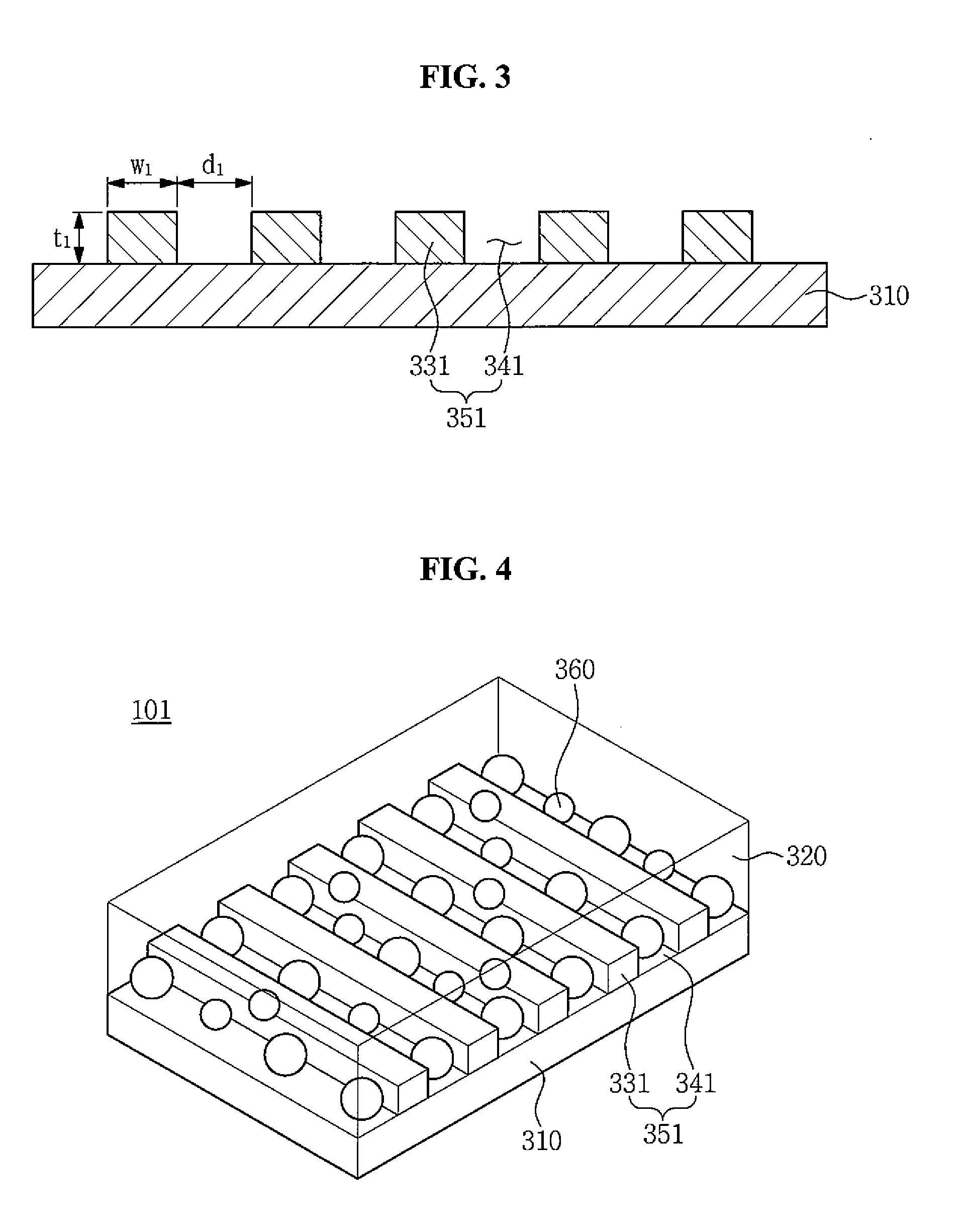
[0054]Hereinafter, embodiments of the present invention will now be described in more detail with reference to the accompanying drawings.

[0055]Advantages and features of the present invention and methods for achieving them will be made clear from embodiments described below in detail with reference to the accompanying drawings. The present invention may, however, be embodied in many different forms and should not be construed as being limited to the embodiments set forth herein. Rather, these embodiments are provided so that this disclosure will be thorough and complete, and will fully convey the scope of the invention to those skilled in the art. The present invention is merely defined by the scope of the claims. Therefore, well-known constituent elements, operations and techniques are not described in detail in the embodiments in order to prevent an understanding of the present invention from being obscured. Like reference numerals refer to like elements throughout the specificati...


PUM

PropertyMeasurementUnit
widthaaaaaaaaaa
diameteraaaaaaaaaa
particle sizeaaaaaaaaaa

Abstract

An anisotropic conductive film (ACF) including a base film, a support unit on the base film, the support unit defining at least one opening, at least one conductive particle in the opening, and an adhesive layer on the support unit and the conductive particle.

Description

CROSS-REFERENCE TO RELATED APPLICATION[0001]This application claims priority to and the benefit of Korean Patent Application No. 10-2015-0096007, filed on Jul. 6, 2015, with the Korean Intellectual Property Office (KIPO), the entire content of which is incorporated herein by reference.BACKGROUND[0002]1. Field[0003]Aspects of embodiments of the present invention relate to an anisotropic conductive film, to a method of manufacturing the anisotropic conductive film, and to a display device including the anisotropic conductive film.[0004]2. Description of the Related Art[0005]Display devices are classified into liquid crystal display (“LCD”) devices, organic light emitting diode (“OLED”) display devices, plasma display panel (“PDP”) devices, electrophoretic display (“EPD”) devices, and the like, based on a light emitting scheme thereof.[0006]In general, the display device includes a display panel for displaying an image and a circuit member for driving the display panel. The circuit mem...

Claims


Application Information

Patent Timeline
Patent Type & Authority Applications(United States)
IPC IPC(8): H05K3/02H05K3/46H05K1/11H05K1/02H01L23/00H05K1/18C09J7/29
CPCH05K3/027H01L24/83H05K1/181H05K1/111H05K1/028H05K2203/107H01L2224/83851H05K2201/032H05K2201/05H05K2203/0514H05K3/4644H01L2224/2949H01L2224/271H01L2224/2939H01L24/16H01L24/27H01L24/29H01L24/32H01L24/73H01L24/81H01L24/92H01L2224/16227H01L2224/2712H01L2224/29005H01L2224/29011H01L2224/29076H01L2224/29078H01L2224/29082H01L2224/2929H01L2224/32227H01L2224/73204H01L2224/81191H01L2224/83101H01L2224/83191H01L2224/83203H01L2224/83862H01L2224/8388H01L2224/9211H01L2224/27003H01L2224/294H01L2224/29486H01L2224/81903H01L2224/2711C08K2201/001C09J2203/318G02F1/1345H05K1/189H05K3/323H05K2201/10136C09J7/29C09J2301/16C09J2301/122C09J2301/314C09J2301/41H01L2924/00012H01L2924/00014H01L2224/81H01L2224/83H01L2224/16225H01L2224/32225H01L2924/00
Inventor KIM, MINSEOKKANG, YEONILKIM, SUNWOONGCHO, YOUNGMINJO, YUNHWAN
Owner SAMSUNG DISPLAY CO LTD
Why Eureka
Try Eureka