Touch display panel
- Summary
- Abstract
- Description
- Claims
- Application Information
AI Technical Summary
Benefits of technology
Problems solved by technology
Method used
Image

Examples
embodiment 1
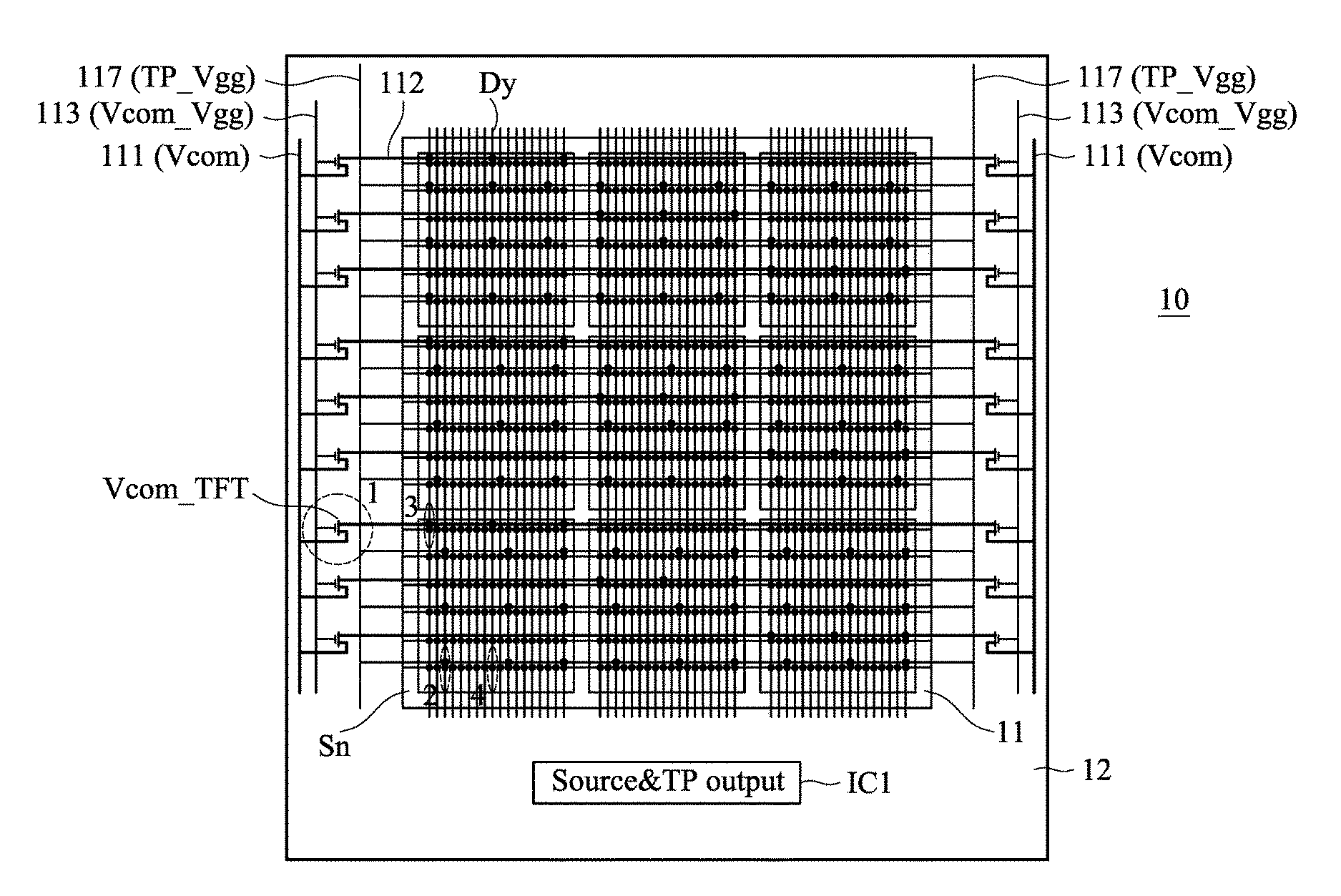
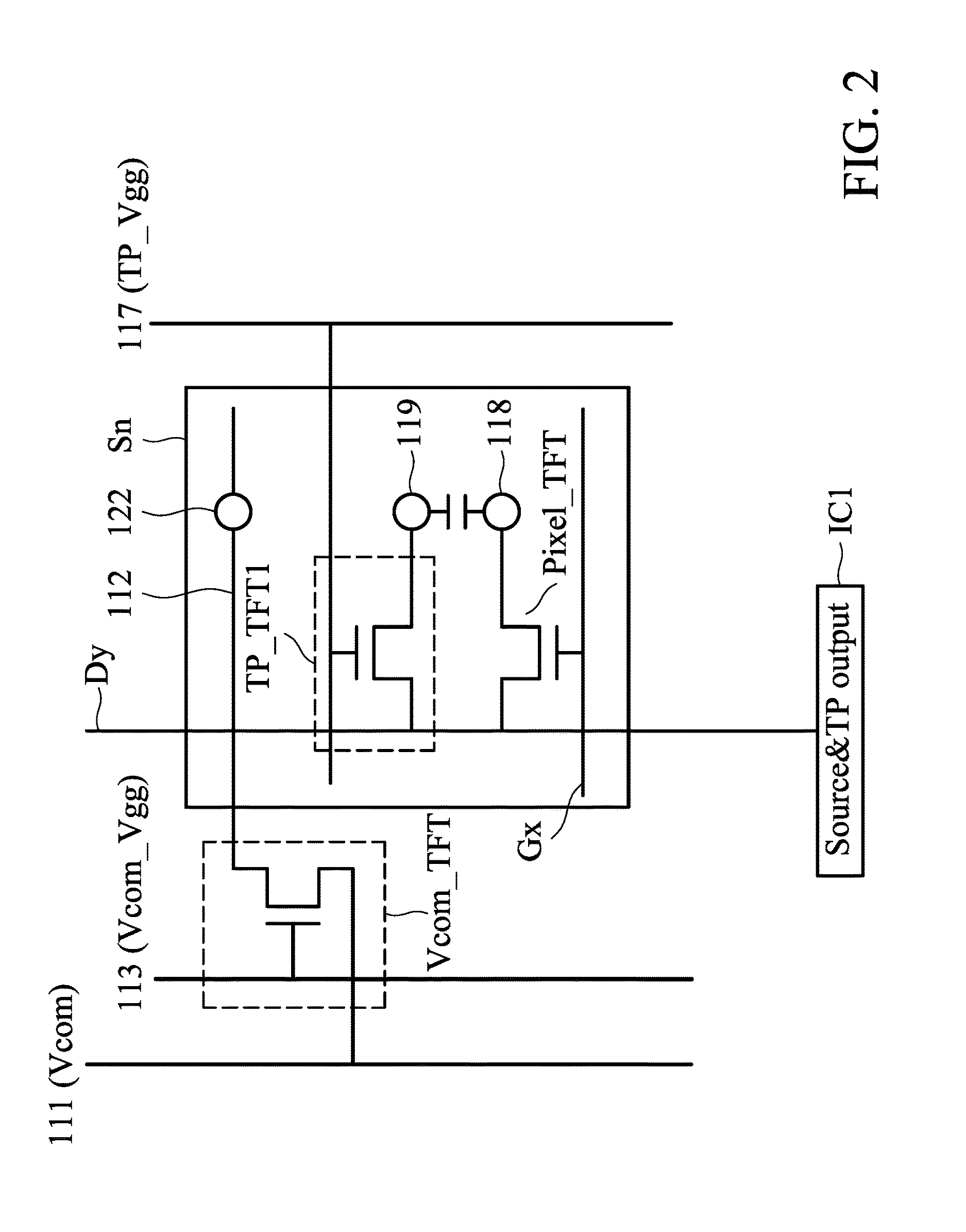
[0047]FIG. 1 is a schematic top view of a touch display panel in accordance with Embodiment 1 of the disclosure. The touch display panel 10 shown in FIG. 1 has a display area 11 and a peripheral area 12 surrounding the display area 11. There are 9 (the number is merely an example) common electrodes (or touch electrodes) Sn. A driving chip IC1 is disposed on the peripheral area 12 and connects with pixels arranged on each pixel columns via data lines Dy. The features of the disclosure can be understood form FIG. 1 by observing four areas respectively labeled with 1˜4. FIG. 2 is an equivalent circuit diagram showing the features of the four areas shown in FIG. 1.
[0048]There are first switching elements Vcom_TFT disposed at the left and right sides of the peripheral area 12. An end of the first switching elements Vcom_TFT is connected to a wire 111 supplying a common voltage level Vcom, and the other end is connected to a common electrode line 112. The common electrode line 112 extends...
embodiment 2
[0059]FIG. 10 is a schematic top view of a touch display panel in accordance with Embodiment 2 of the disclosure. In the touch display panel 20 shown in FIG. 10, the output terminal (channel) of the driving chip IC2 is different from the driving chip IC1. There is a fourth switching element TP_TFT2 disposed between the output terminal of the driving chip IC2 and the data line Dy. The other features of the touch display panel 20 are the same as the touch display panel 10. The detailed features of the touch display panel 20 are shown in FIG. 11.
[0060]FIG. 11 is an equivalent circuit diagram showing the features of multiple areas shown in FIG. 10. In Embodiment 2, the driving chip IC2 includes two portions: a data signal output portion (the part labeled “Source output” in FIG. 11) and a touch sensing signal portion (the part labeled “TP output” in FIG. 11). The data signal output portion has output terminals for outputting the data signals, the number of which is the same as the number...
PUM
 Abstract
Description
Claims
Application Information