Electron Microscope and Measurement Method

a technology of electron microscope and measurement method, which is applied in the direction of basic electric elements, electric discharge tubes, electrical apparatus, etc., can solve the problems of deteriorating positional resolution and more difficult to measure the amount of deflection of electron beam eb with high sensitivity, and achieve high positional resolution and high sensitivity

Active Publication Date: 2017-01-26
THE UNIV OF TOKYO +1
View PDF2 Cites 2 Cited by
  • Summary
  • Abstract
  • Description
  • Claims
  • Application Information

AI Technical Summary

Benefits of technology

[0029]In this measurement method, the camera length is so adjusted that the periphery of the cross section of the transmitted electron beam lies within the detection surface, the beam being emitted from the sample in response to impingement of the central portion of the cross section of the beam on the sample. Consequently, the amount of deflection of the beam occurring when it is transmitted through the sample can be measured with high sensitivity and high positional resolution.

Problems solved by technology

Consequently, it is more difficult to measure the amount of deflection of the electron beam EB with high sensitivity.
Nonetheless, the angle of convergence decreases and so diffraction deteriorates the positional resolution.

Method used


Image

  • Electron Microscope and Measurement Method
  • Electron Microscope and Measurement Method
  • Electron Microscope and Measurement Method

Examples


first embodiment

1. First Embodiment

1.1. Electron Microscope

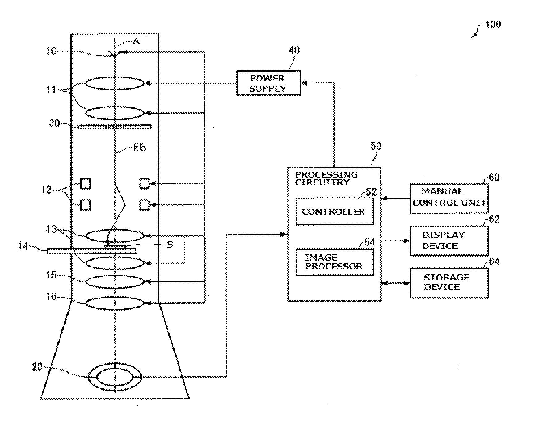
[0046]An electron microscope associated with a first embodiment of the present invention is first described by referring to FIG. 1, which schematically shows the configuration of the electron microscope, 100.

[0047]In the electron microscope 100, an amount of deflection of an electron beam EB occurring when it is transmitted through a sample S can be measured. Electromagnetic fields within the sample that cause the deflection of the beam can be computed from the results of the measurement by a DPC (differential phase contrast) method.

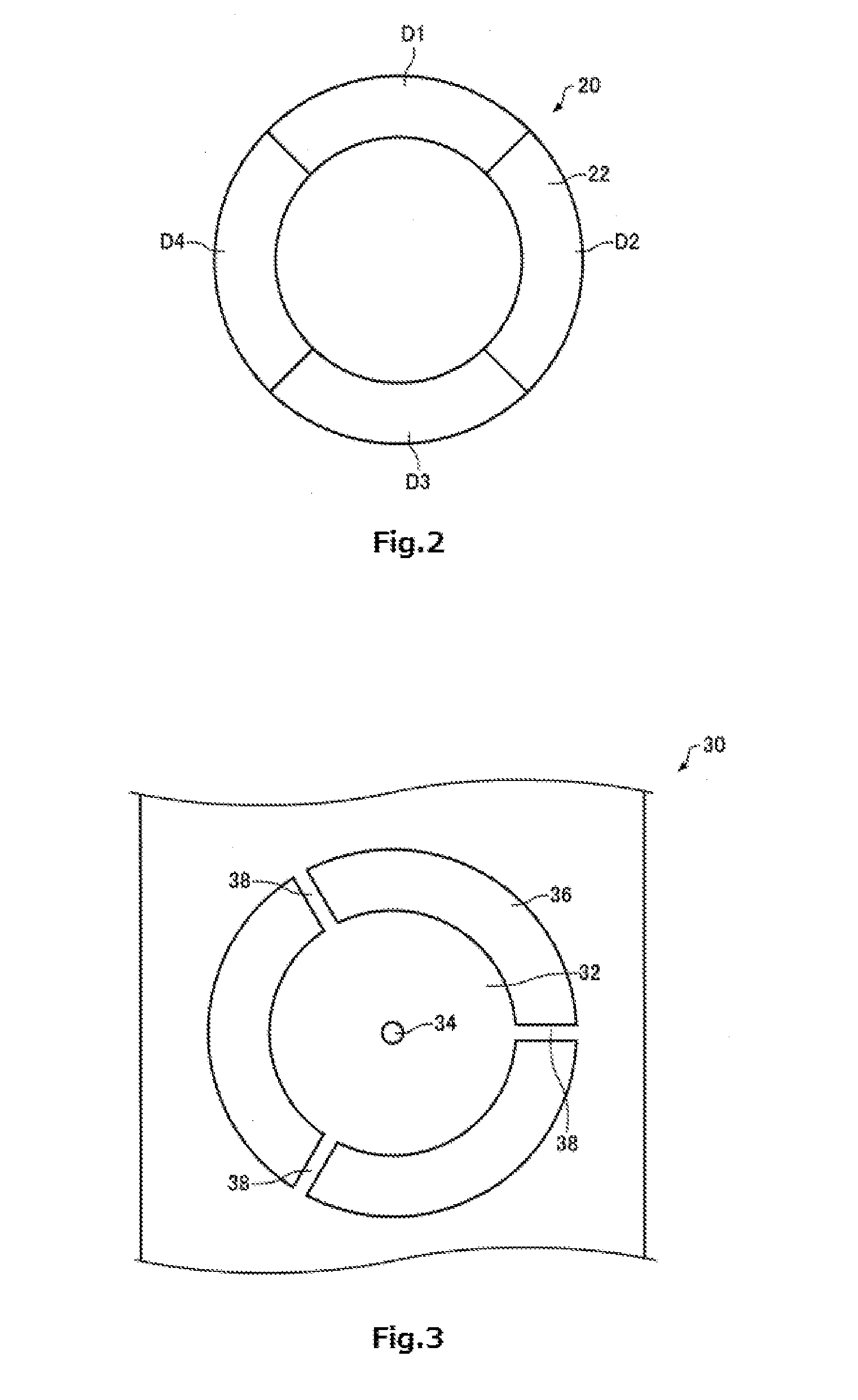
[0048]As shown in FIG. 1, the electron microscope 100 includes an electron beam source 10, an illumination lens system 11, a deflector 12, an objective lens 13, a sample stage 14, an intermediate lens 15, a projector lens 16, a segmented detector 20, a condenser aperture 30, a power supply 40, processing circuitry 50, a manual control unit 60, a display device 62, and a storage device 64.

[0049]The electron beam ...

second embodiment

2. Second Embodiment

2.1. Electron Microscope

[0090]An electron microscope associated with a second embodiment is next described by referring to FIG. 7, which schematically shows the configuration of the electron microscope, 200, associated with the second embodiment. Those members of the electron microscope 200 associated with the second embodiment which are similar in function with their respective counterparts of the electron microscope 100 associated with the first embodiment are indicated by the same reference numerals as in the above referenced figures and a detail description thereof is omitted.

[0091]As shown in FIG. 7, the electron microscope 200 differs from the above-described electron microscope 100 in that it has a dark field detector 210 and a camera length control lens system 220.

[0092]The dark field detector 210 detects scattered and diffracted electrons out of electrons transmitted through the sample S. For example, the dark field detector 210 is an annular dark-field ...

third embodiment

3. Third Embodiment

3.1. Electron Microscope

[0102]An electron microscope associated with a third embodiment is next described by referring to FIG. 9, which schematically shows the configuration of the electron microscope, 300, associated with the third embodiment. Those members of the electron microscope 300 associated with the third embodiment which are similar in function to their respective counterparts of the electron microscope 100 associated with the first embodiment are indicated by the same reference numerals as in the above referenced figures and a detail description thereof is omitted.

[0103]As shown in FIG. 9, the electron microscope 300 differs from the above-described electron microscope 100 in that the condenser aperture 30 is composed of a first aperture portion 310 and a second aperture portion 320. That is, the condenser aperture 30 comprises two stages of aperture portions, i.e., the first aperture portion 310 on the front side and the second aperture portion 320 on ...


PUM


Abstract

An electron microscope is provided which can measure, with high sensitivity and high positional resolution, an amount of deflection of an electron beam occurring when it is transmitted through a sample. The electron microscope (100) is adapted to measure the amount of deflection of the electron beam (EB) when it is transmitted through the sample (S), and has an electron beam source (10) producing the electron beam (EB), an illumination lens system for focusing the electron beam (EB) onto the sample (S), an aperture (30) having an electron beam blocking portion (32) for providing a shield between a central portion (EB1) and an outer peripheral portion (EB2) of the cross section of the beam (EB) impinging on the sample (S), and a segmented detector (20) having a detection surface (22) for detecting the electron beam (EB) transmitted through the sample (S). The detection surface (22) is divided into a plurality of detector segments (D1-D4).

Description

BACKGROUND OF THE INVENTION[0001]Field of the Invention[0002]The present invention relates to an electron microscope and measurement method.[0003]Description of Related Art[0004]In scanning transmission electron microscopy (STEM), the differential phase contrast (DPC) method is known as a technique for visualizing electromagnetic fields. In this technique, an amount of deflection occurring when an electron beam is transmitted through a sample is measured, and the electromagnetic field present within the sample that causes the deflection of the beam is calculated (see, for example, JP-A-2009-277618).[0005]FIG. 13 schematically illustrates the operation of a conventional electron microscope, 101, performed when measurements are made by the DPC method using a segmented detector 104. Note that FIG. 13 shows only main portions of the electron microscope 101. FIG. 14 is a schematic representation of the segmented detector 104.[0006]As shown in FIG. 13, an electron beam EB produced by an e...

Claims


Application Information

Patent Timeline
Patent Type & Authority Applications(United States)
IPC IPC(8): H01J37/244H01J37/22H01J37/09H01J37/26
CPCH01J37/244H01J37/26H01J2237/24578H01J37/09H01J2237/0453H01J37/226H01J37/28H01J2237/2614H01J2237/2802
Inventor SHIBATA, NAOYAKOHNO, YUJISAWADA, HIDETAKA
Owner THE UNIV OF TOKYO
Why Eureka
Try Eureka