

Semiconductor process for treating metal gate
- Summary
- Abstract
- Description
- Claims
- Application Information
AI Technical Summary
Benefits of technology
Problems solved by technology
Method used
Image

Examples
Embodiment Construction
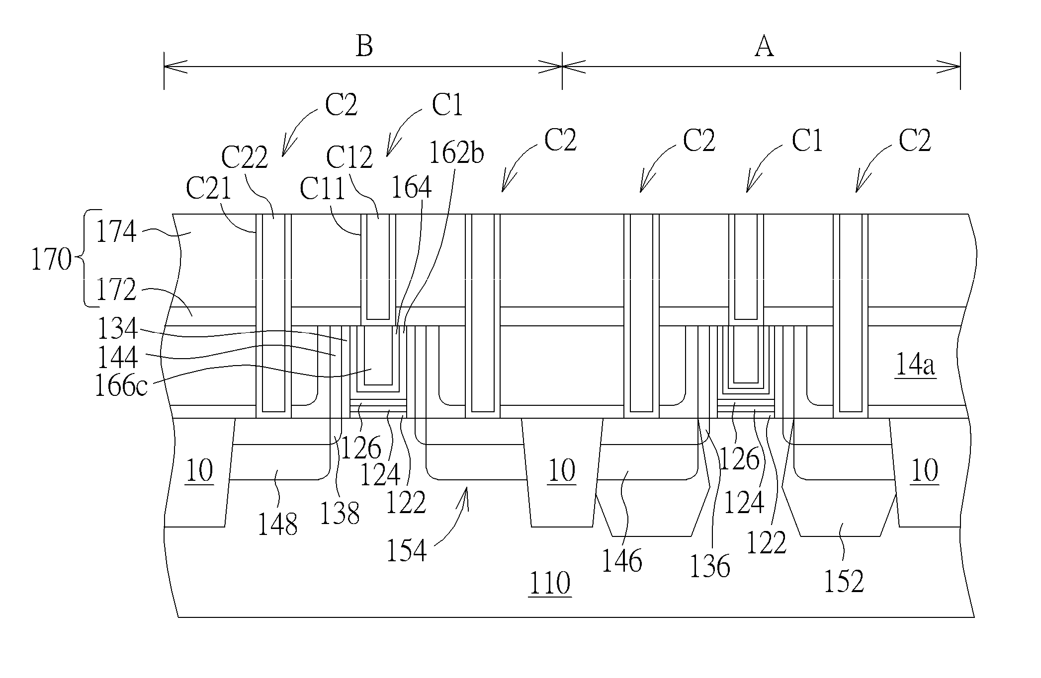
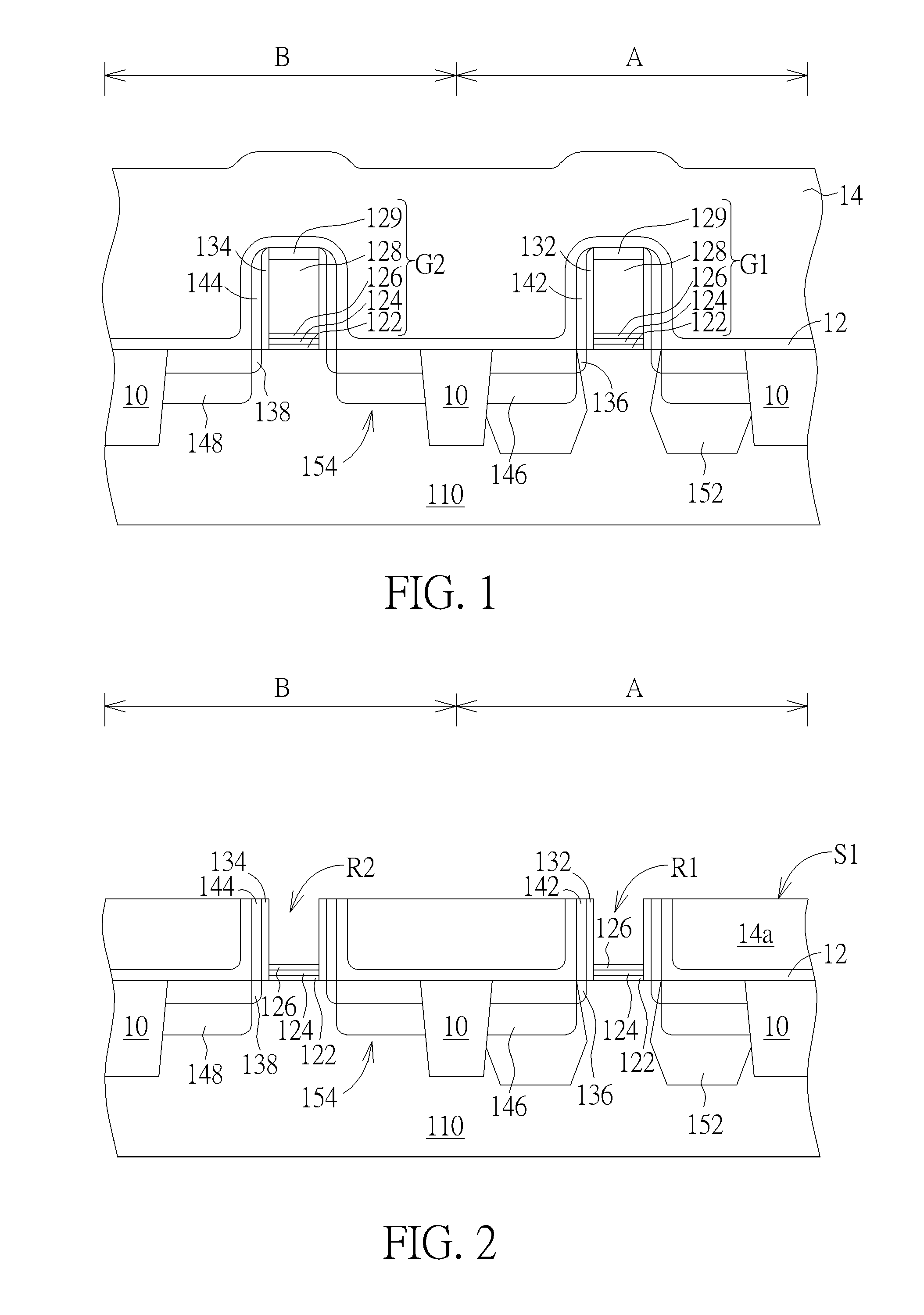
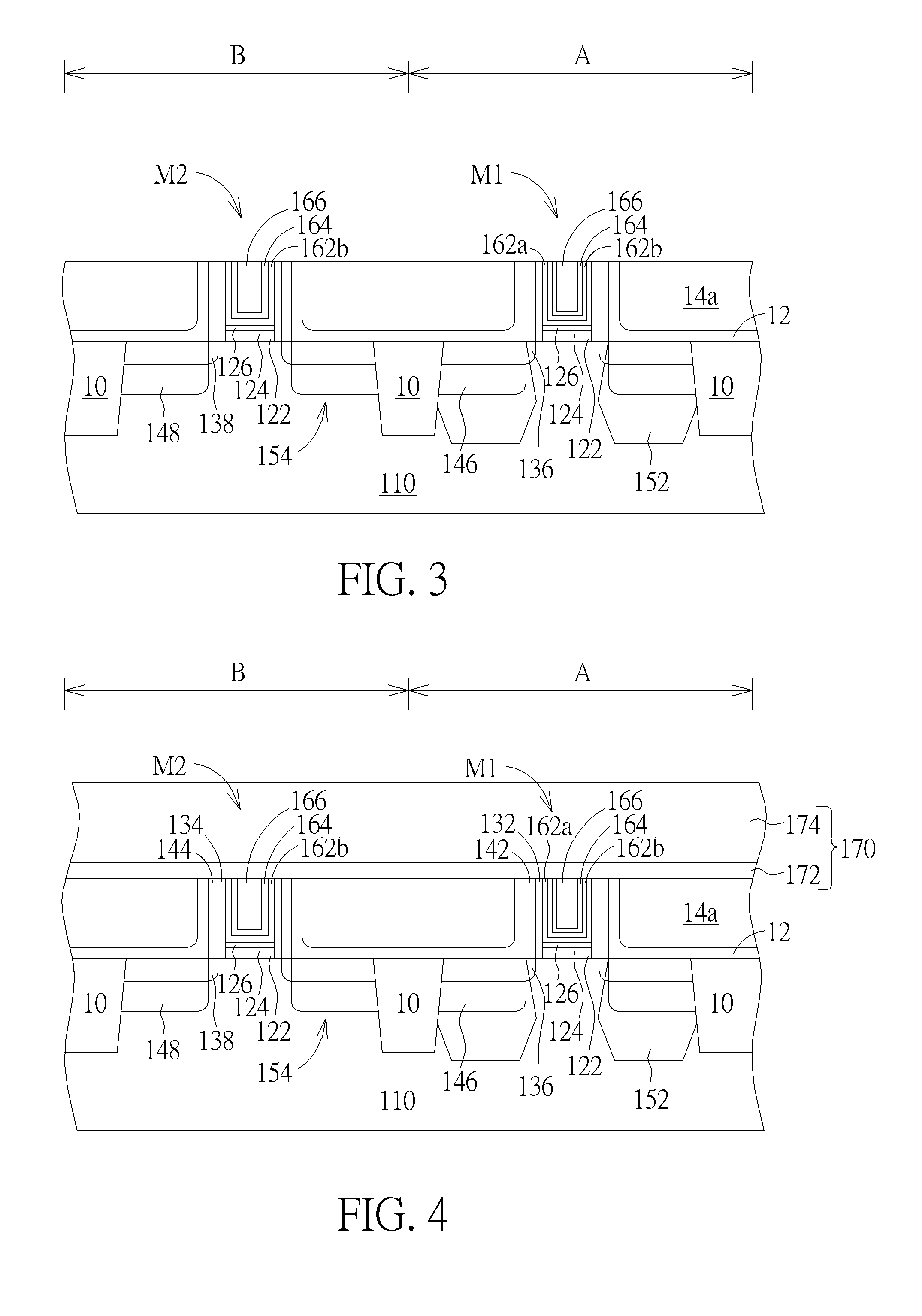
[0013]A semiconductor process of the present invention is applied to a CMOS transistor having a PMOS transistor paired with an NMOS transistor in the following embodiment. However, the present invention is not restricted thereto. The present invention can also be applied to a MOS transistor such as a planar MOS transistor, a non-planar MOS transistor, or others, depending upon practical requirements.
[0014]FIGS. 1-8 schematically depict cross-sectional views of a semiconductor process for treating a metal gate according to an embodiment of the present invention. As shown in FIG. 1, a substrate 110 is provided. The substrate 110 may be a semiconductor substrate such as a silicon substrate, a silicon containing substrate, a III-V group-on-silicon (such as GaN-on-silicon) substrate, a graphene-on-silicon substrate or a silicon-on-insulator (SOI) substrate. Isolation structures 10 may be formed in the substrate 110 to electrically isolate each transistor. The isolation structures 10 may ...
PUM
 Abstract
Description
Claims
Application Information