Method for manufacturing coa liquid crystal panel and coa liquid crystal panel

a liquid crystal panel and liquid crystal panel technology, applied in non-linear optics, instruments, optics, etc., can solve the problems of loss of a large fraction of aperture ratio, and achieve the effect of increasing aperture ratio and simplifying manufacturing process

Active Publication Date: 2017-02-16
TCL CHINA STAR OPTOELECTRONICS TECH CO LTD
View PDF4 Cites 6 Cited by
  • Summary
  • Abstract
  • Description
  • Claims
  • Application Information

AI Technical Summary

Benefits of technology

[0008]An object of the present invention is to provide a method for manufacturing a color filter on array (COA) liquid crystal panel, which simplifies the manufacturing process and increases aperture ratio.

Problems solved by technology

Liquid crystal that is located above the intersection zone may suffer incorrect orientation due to terrain variation and thus needs a black matrix of a large area to be formed on one side of the glass substrate for shielding.
However, the arrangement of the black matrix of a large area causes a loss of a large fraction of aperture ratio.

Method used


Image

  • Method for manufacturing coa liquid crystal panel and coa liquid crystal panel
  • Method for manufacturing coa liquid crystal panel and coa liquid crystal panel
  • Method for manufacturing coa liquid crystal panel and coa liquid crystal panel

Examples


Embodiment Construction

[0051]To further expound the technical solution adopted in the present invention and the advantages thereof, a detailed description is given to a preferred embodiment of the present invention and the attached drawings.

[0052]Referring to FIG. 1, the present invention provides a method for manufacturing a color filter on array (COA) liquid crystal panel, which comprises the following steps:

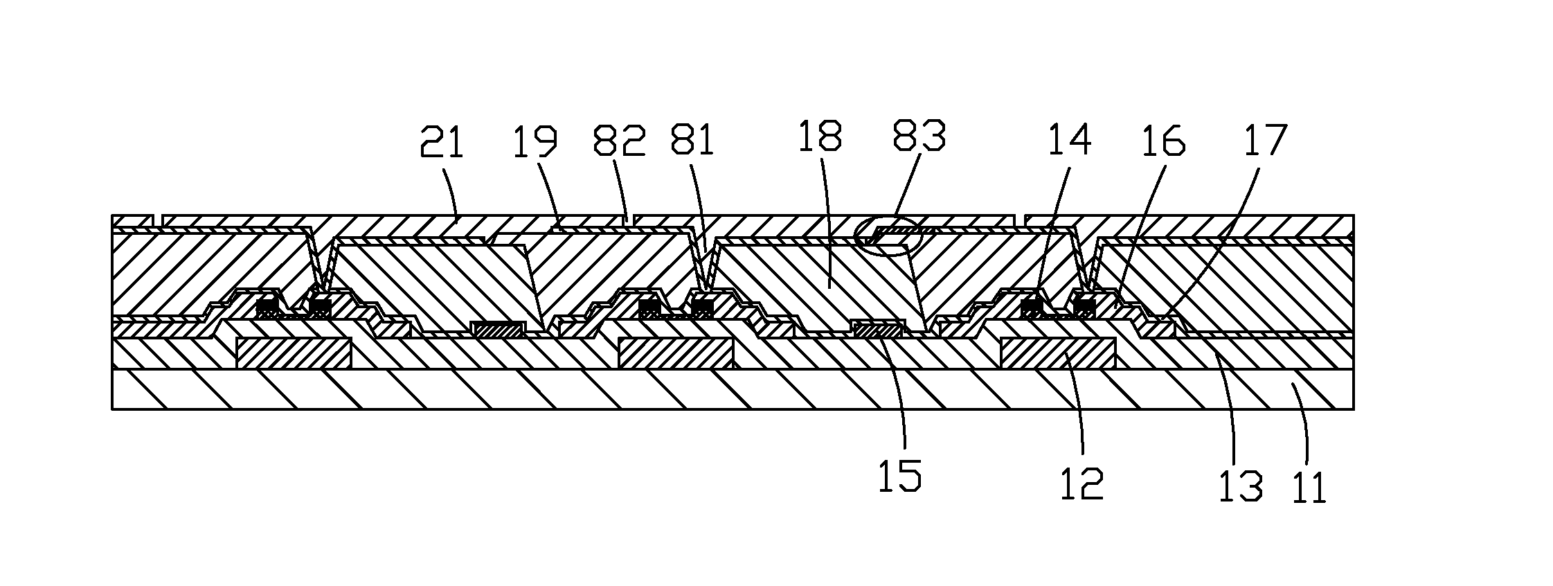
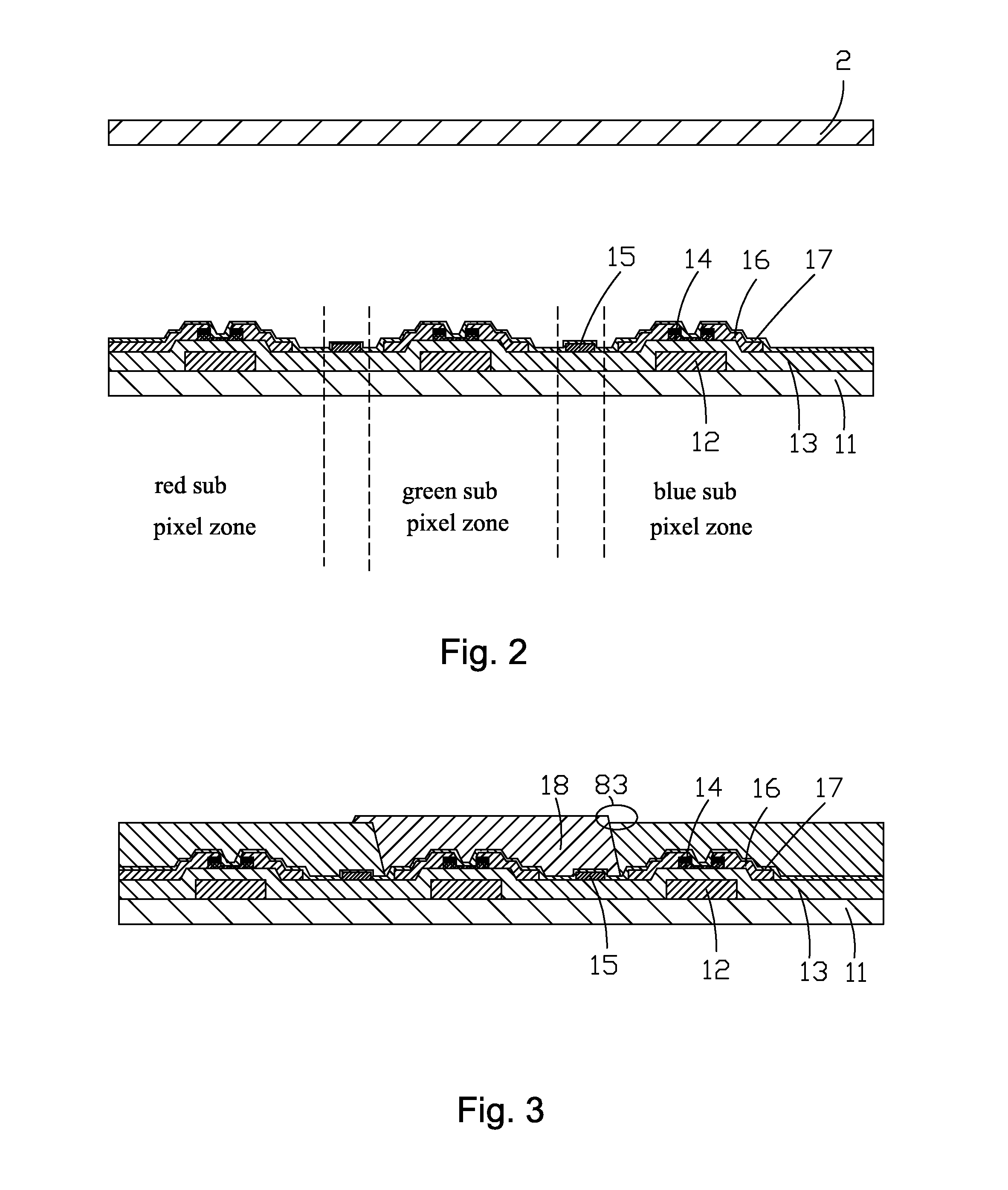
[0053]Step 1: as shown in FIG. 2, providing an array substrate 1 and a glass substrate 2.

[0054]Specifically, the array substrate 1 comprises red, green, blue sub pixel zones. Each of the sub pixel zones comprises a base plate 11, a gate terminal 12 and a scan line arranged on the base plate 11, a gate insulation layer 13 arranged on the gate terminal 12 and covering the base plate 11, a semiconductor layer 14 arranged on the gate insulation layer 13 and located above the gate terminal 12, source / drain terminals 16 arranged on the gate insulation layer 13 and respectively in connection with two ends ...


PUM

PropertyMeasurementUnit
transparentaaaaaaaaaa
metallicaaaaaaaaaa
parasitic capacitanceaaaaaaaaaa

Abstract

The present invention provides a method for manufacturing a COA liquid crystal panel and a COA liquid crystal panel. The method includes forming a first pixel electrode layer on a color resist layer, forming a planarization layer on the first pixel electrode layer, and forming a second pixel electrode layer that is in engagement with the first pixel electrode layer on the planarization layer so as to achieve planarization of the pixel electrode layer to the maximum extent. Further, the second pixel electrode layer includes a pixel electrode block that is located in each sub pixel zone and has a lateral border located above a scan line and a longitudinal border located above a signal line so as to achieve self-shielding of light for the scan line and the signal line, allowing for omission of lateral and longitudinal black matrixes. Further, a dot-like black matrix is formed on a glass substrate at a location corresponding to a TFT on the array substrate to shield light for a site of a channel thereby simplifying the manufacturing process and increase the aperture ratio.

Description

BACKGROUND OF THE INVENTION[0001]1. Field of the Invention[0002]The present invention relates to the field of display technology, and in particular to a method for manufacturing a color filter on array (COA) liquid crystal panel and a COA liquid crystal panel.[0003]2. The Related Arts[0004]Liquid crystal displays (LCDs) have a variety of advantages, such as thin device body, low power consumption, and being free of radiation, and are thus of wide applications, such as liquid crystal televisions, mobile phones, personal digital assistants (PDAs), digital cameras, computer monitors, and notebook computer screens.[0005]A liquid crystal display generally comprises an enclosure, a liquid crystal panel arranged in the enclosure, and a backlight module mounted in the enclosure. The liquid crystal panel has a structure that is composed of a thin-film transistor (TFT) array substrate, a color filter (CF) substrate, and a layer of liquid crystal arranged between the two substrates and the ope...

Claims


Application Information

Patent Timeline
Patent Type & Authority Applications(United States)
IPC IPC(8): G02F1/1368G02F1/1343G02F1/1362
CPCG02F1/1368G02F1/136286G02F1/13439G02F1/136227G02F2001/133302G02F2201/121G02F2001/136295G02F2201/123G02F2001/133357G02F2201/52G02F2202/02G02F2001/136222G02F1/1333G02F1/134309G02F1/136209G02F1/133357G02F1/136222G02F1/133302G02F1/136295G02F1/1335G02F1/1343
Inventor XU, HONGYUANSUN, BO
Owner TCL CHINA STAR OPTOELECTRONICS TECH CO LTD
Why Eureka
Try Eureka