Gas supply nozzle, substrate processing apparatus, and non-transitory computer-readable recording medium

a substrate processing and gas supply technology, applied in the direction of coatings, chemical vapor deposition coatings, metallic material coating processes, etc., can solve the problem of difficult uniform formation of films on substrates, and achieve the effect of improving the uniformity of film thicknesses on substrates

Active Publication Date: 2017-02-23
KOKUSA ELECTRIC CO LTD
View PDF1 Cites 324 Cited by
  • Summary
  • Abstract
  • Description
  • Claims
  • Application Information

AI Technical Summary

Benefits of technology

[0007]According to the present invention, it is possible to improve film thickness uniformity among substrates.

Problems solved by technology

However, in recent years, since such a semiconductor device has a tendency to be highly integrated and the pattern size has been remarkably miniaturized, it has been difficult to uniformly form films on a substrate.

Method used


Image

  • Gas supply nozzle, substrate processing apparatus, and non-transitory computer-readable recording medium
  • Gas supply nozzle, substrate processing apparatus, and non-transitory computer-readable recording medium
  • Gas supply nozzle, substrate processing apparatus, and non-transitory computer-readable recording medium

Examples


first embodiment

[0023]Hereinafter, an embodiment of the present invention will be described with reference to FIGS. 1 to 3.

[0024](1) Configuration of Substrate-Processing Apparatus

[0025](Heating Unit)

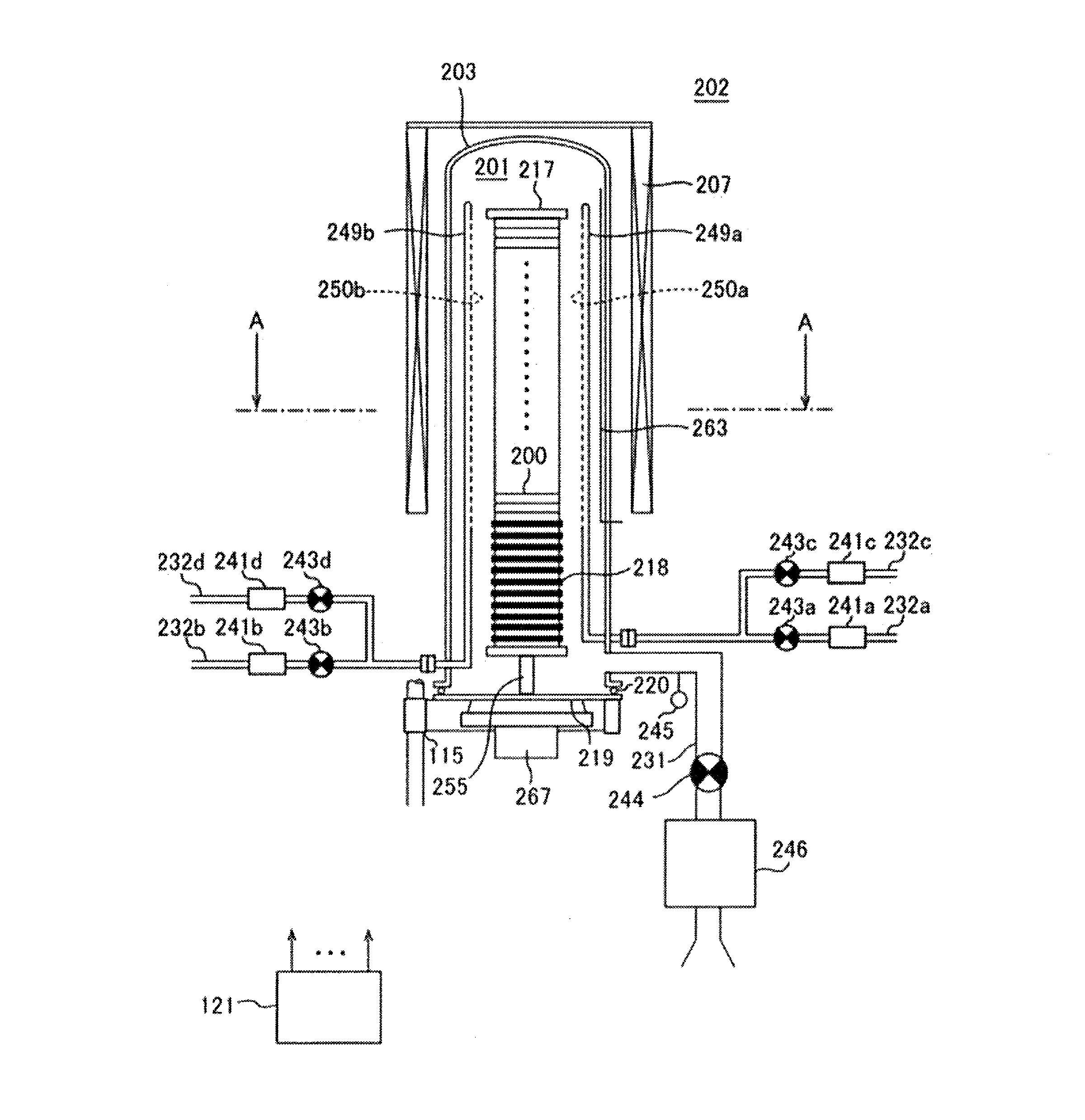
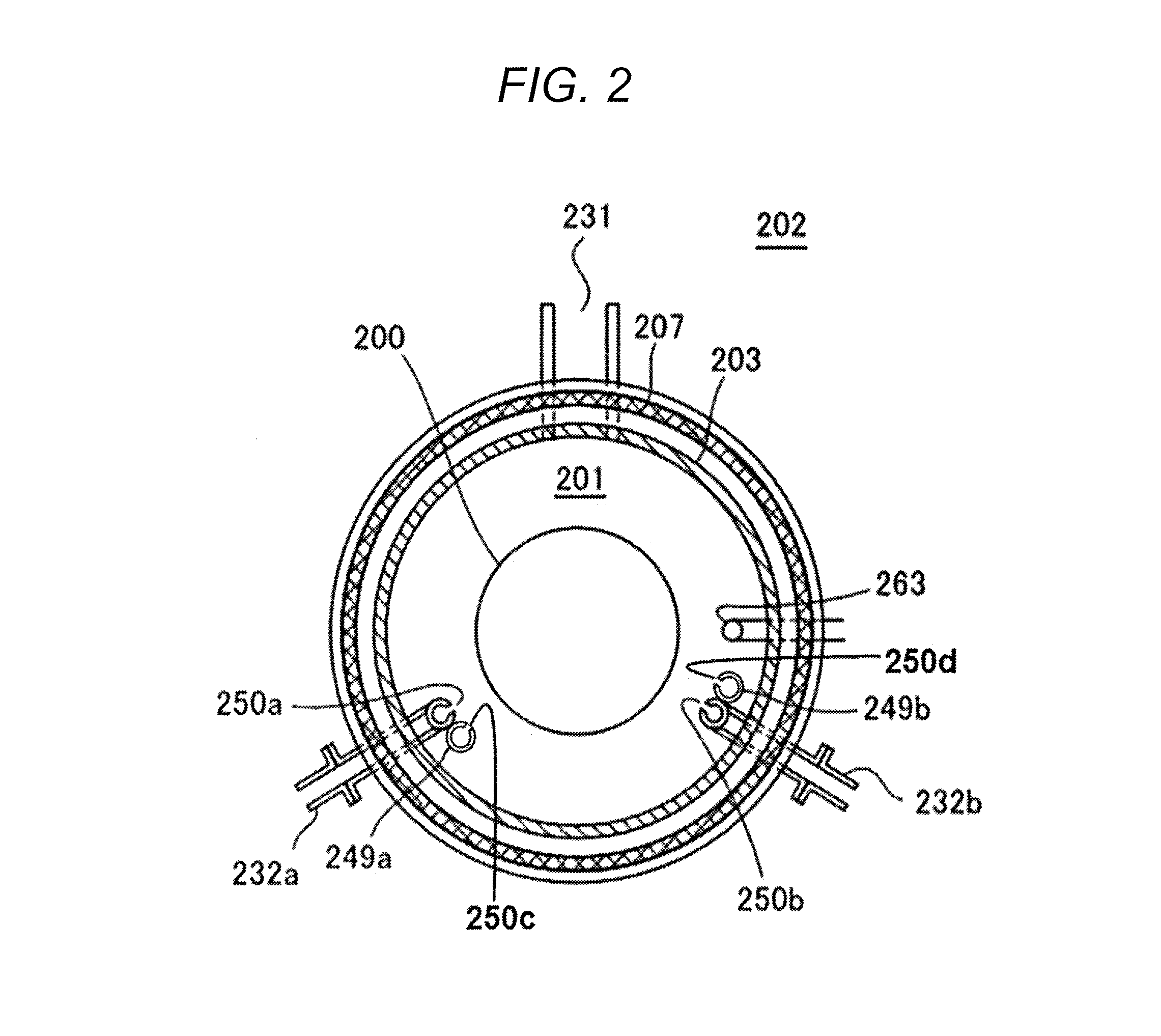
[0026]As illustrated in FIG. 1, a processing furnace 202 includes a heater 207 as a heating unit (heating mechanism). The heater 207 has a cylindrical shape and is vertically installed by being supported by a heater base (not shown) as a holding plate. The heater 207 also functions as an activating mechanism (excitation unit) of activating (exciting) a gas by heat as described later.

[0027]A reaction tube 203 constituting a reaction container (process container) is installed inside the heater 207 to be concentric with the heater 207. The reaction tube 203 is made of a heat resistant material such as quartz (SiO2) or silicon carbide (SiC) and is formed in a cylindrical shape of which top end is closed and of which bottom end is opened. A processing chamber 201 is formed in a cylindrical hollow portion of...

modified example

[0172]Next, modified Examples of the present invention will be described with reference to FIGS. 10A to 10C. As illustrated in FIGS. 10A, 10B, and 10C, the gas supply holes 250 are provided to both of the upstream side pipe 271-1 and the downstream side pipe 271-2 of the nozzle 249, and as illustrated in FIG. 10D, the gas supply holes 250 are provided to only the downstream side pipe 271-2, and thus, the processing gas activated by heating is easily supplied on the wafer 200, so that it is possible to obtain the effect that it is possible to improve the inter-plane film thickness uniformity between the wafers.

[0173]In addition, as illustrated in FIG. 10E, the gas supply holes 250 are provided to only the upstream side pipe 271-1, and thus, even in a case where by-products such as particles inside the nozzle occur, since the gas supply holes 250 are not provided to the downstream side pipe 271-2, it is possible to obtain the effect that it is possible to easily exhaust the by-product...

second embodiment

[0177]Next, a second embodiment of the present invention will be described with reference to FIGS. 11 and 12. A substrate processing apparatus according to the second embodiment is different from that of the first embodiment in that, as illustrated in FIG. 11, the nozzle 249a supplying the source gas is arranged as a U-shaped nozzle, and instead of the nozzle 249b illustrated in FIGS. 1 and 2, a nozzle supplying the reaction gas or the inert gas is arranged as a straight-pipe-type nozzle 251. The other configurations are the same as those of the first embodiment.

[0178]In addition, as illustrated in FIG. 12, only the nozzle 249a supplying a source gas which needs to be activated by heating is arranged as a U-shaped nozzle, so that it is possible to facilitate maintenance, and it is possible to reduce device cost.

[0179]By the configuration according to the second embodiment, it is possible to obtain the following effects.

[0180](g) The number of U-shaped nozzles of which structure is c...


PUM

PropertyMeasurementUnit
flow velocityaaaaaaaaaa
pressureaaaaaaaaaa
pressureaaaaaaaaaa

Abstract

Provided is a technology including a nozzle base end portion which is provided in a processing chamber processing a substrate to extend in a vertical direction and into which a processing gas processing the substrate is introduced, a nozzle distal end portion which is configured in a U shape and in which a gas supply hole supplying the processing gas is provided to a side surface of the substrate, and a gas residence suppressing hole which is provided in a downstream end of the nozzle distal end portion and has a diameter larger than that of the gas supply hole.

Description

BACKGROUND OF THE INVENTION[0001]Field of the Invention[0002]The present invention relates to a gas supply nozzle, a substrate processing apparatus, a method of manufacturing a semiconductor device, and a program.[0003]Description of the Related Art[0004]As one process of a process of manufacturing a semiconductor device, in some cases, a process of forming films on substrates is performed by non-simultaneously supplying a source gas and a reaction gas to multiple stages of the substrates arranged in a processing chamber.SUMMARY OF THE INVENTION[0005]However, in recent years, since such a semiconductor device has a tendency to be highly integrated and the pattern size has been remarkably miniaturized, it has been difficult to uniformly form films on a substrate. The present invention is to provide a technique capable of improving film thickness uniformity among substrates.[0006]According to an aspect of the present invention, there is provided a technology including: a nozzle base e...

Claims


Application Information

Patent Timeline
Patent Type & Authority Applications(United States)
IPC IPC(8): C23C16/455H01L21/02C23C16/24
CPCC23C16/45563C23C16/24H01L21/02186H01L21/02189H01L21/02271H01L21/02183H01L21/02178H01L21/02175H01L21/02181H01L21/205C23C16/45578H01L21/31H01L21/67011H01L21/02126H01L21/02211H01L21/0228C23C16/30C23C16/455C23C16/45531H01L21/02263H01L21/02312H01L21/02337H01L21/54
Inventor TAKAGI, KOSUKESASAJIMA, RYOTAKOGURA, SHINTAROAKAE, NAONORIYAMAKOSHI, RISAFUJINO, TOSHIKITERASAKI, MASATOMINAMI, MASAYOSHI
Owner KOKUSA ELECTRIC CO LTD
Why Eureka
Try Eureka