Method for modulating work function of semiconductor device having metal gate structure by gas treatment

a technology of metal gate structure and work function, which is applied in the direction of semiconductor/solid-state device manufacturing, basic electric elements, electric apparatus, etc., can solve the problems of difficult control of process stability, increase threshold voltage, and form a continuous film, and achieve the effect of simple process

Active Publication Date: 2017-03-16
UNITED MICROELECTRONICS CORP
View PDF2 Cites 14 Cited by
  • Summary
  • Abstract
  • Description
  • Claims
  • Application Information

AI Technical Summary

Benefits of technology

[0008]The invention provides a method for modulating a work function of a semiconductor device having a metal g

Problems solved by technology

Thus, threshold voltage increases, and the performance of the device is affected accordingly.
However, under the condition where the work function of the semiconductor device is modulated through the

Method used


Image

  • Method for modulating work function of semiconductor device having metal gate structure by gas treatment
  • Method for modulating work function of semiconductor device having metal gate structure by gas treatment
  • Method for modulating work function of semiconductor device having metal gate structure by gas treatment

Examples


Embodiment Construction

[0034]Referring to the drawings attached, the disclosure will be described by means of the embodiments below. Nevertheless, the disclosure can be embodied in many different forms and should not be construed as limited to the embodiments set forth herein. The language used to describe the directions such as “above”, “below”, “front”, “back”, “inner”, and “external” or the like in the reference drawings should be regarded in an illustrative rather than in a restrictive sense. Thus, the language used to describe the directions is not intended to limit the scope of the disclosure. For the purpose of clarity, the sizes and relative sizes of each of the layers in the drawings can be illustrated in exaggerated proportions.

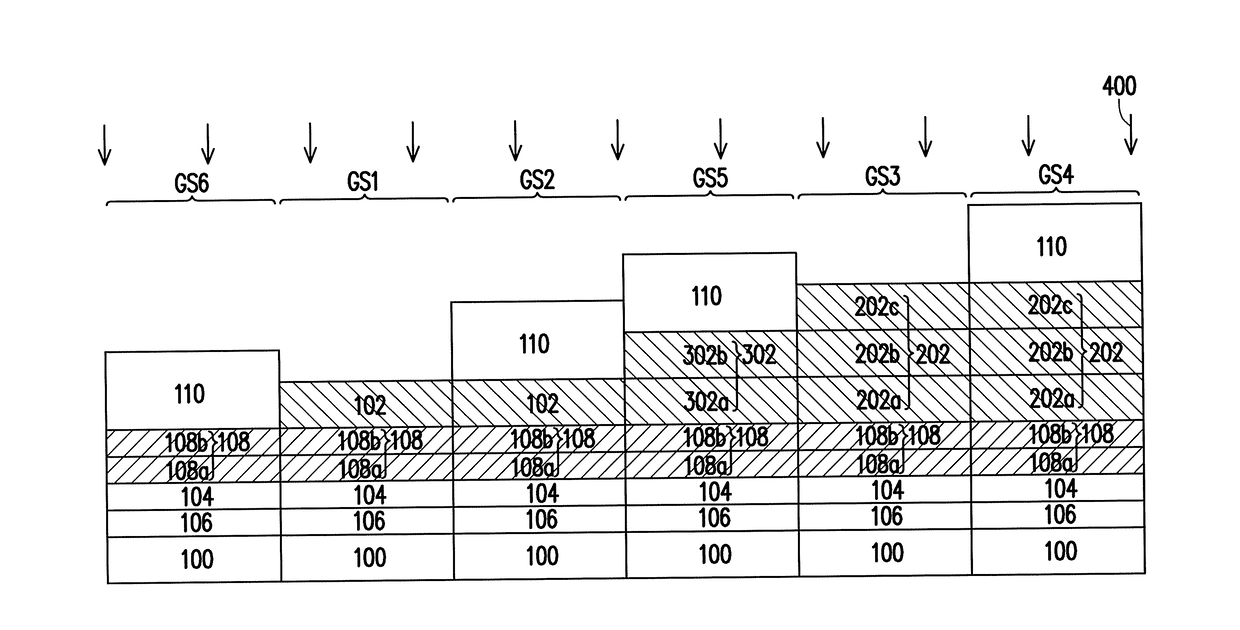
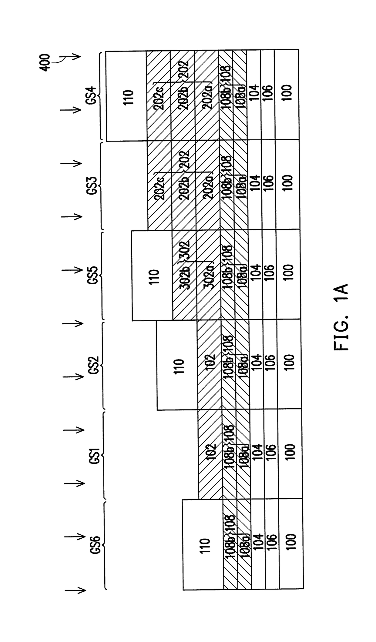
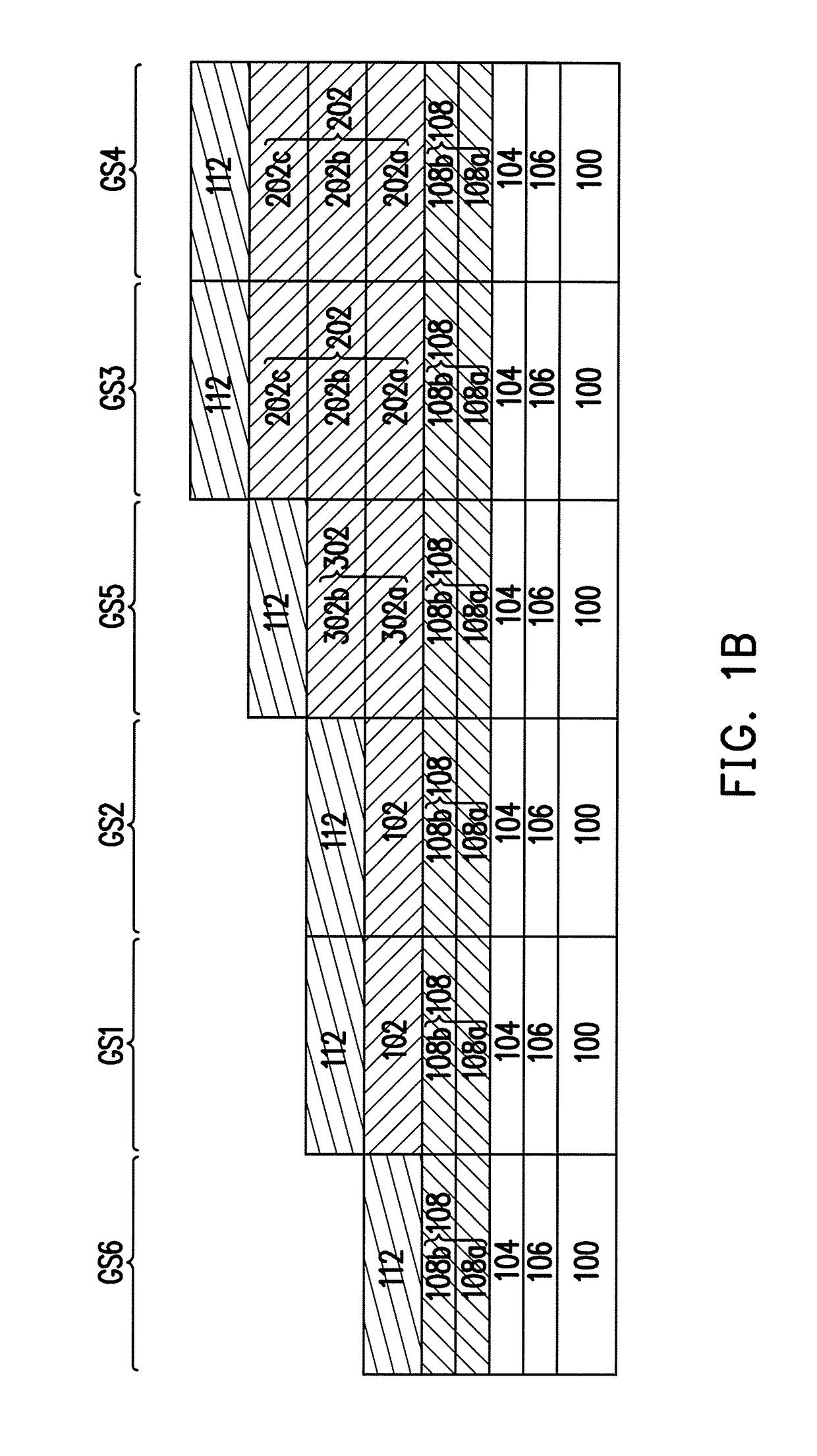
[0035]FIGS. 1A to 1B are sectional schematic views illustrating modulation of a work function of a semiconductor device having a metal gate structure according to an embodiment of the invention. FIG. 2 is a sectional schematic view illustrating a metal gate structure acco...


PUM


Abstract

A method for modulating a work function of a semiconductor device having a metal gate structure including the following steps is provided. A first stacked gate structure and a second stacked gate structure having an identical structure are provided on a substrate. The first stacked gate structure and the second stacked gate structure respectively include a first work function metal layer of a first type. A patterned hard mask layer is formed. The patterned hard mask layer exposes the first work function metal layer of the first stacked gate structure and covers the first work function metal layer of the second stacked gate structure. A first gas treatment is performed to the first work function metal layer of the first stacked gate structure exposed by the patterned hard mask layer. A gas used in the first gas treatment includes nitrogen-containing gas or oxygen-containing gas.

Description

CROSS-REFERENCE TO RELATED APPLICATION[0001]This application claims the priority benefit of China patent application serial no. 201510584677.9, filed on Sep. 15, 2015. The entirety of the above-mentioned patent application is hereby incorporated by reference herein and made a part of the specification.BACKGROUND OF THE INVENTION[0002]Field of the Invention[0003]The invention is related to method for fabricating a semiconductor device, and particularly related to a method for modulating work function of a semiconductor device having a metal gate structure.[0004]Description of Related Art[0005]As the size of a semiconductor device is getting smaller, the size of a gate structure and the thickness of a gate dielectric layer have been reduced. However, leakage current occurs under the condition where the thickness of the gate dielectric layer formed of silicon oxide is reduced. To avoid occurrence of leakage current, the conventional means adopts high dielectric constant (high-k) materi...

Claims


Application Information

Patent Timeline
IPC IPC(8): H01L21/8238
CPCH01L21/823842H01L21/28158H01L21/285
Inventor CHANG, YUN-TZUCHOU, SHIH-MINLAI, KUO-CHIHCHANG, CHING-YUNYEN, HSIANG-CHIEHCHEN, YEN-CHENLU, YANG-JUHO, NIEN-TINGHSU, CHI-MAO
Owner UNITED MICROELECTRONICS CORP
Why Eureka
Try Eureka