III-Nitride Semiconductor Light Emitting Device Having Amber-to-Red Light Emission (>600 nm) and a Method for Making Same

Active Publication Date: 2017-04-13
OSTENDO TECH INC
View PDF8 Cites 5 Cited by
  • Summary
  • Abstract
  • Description
  • Claims
  • Application Information

AI Technical Summary

Problems solved by technology

There are two common reasons for the efficiency loss in III-nitride light emitters: (1) a large lattice mismatch between InGaN and GaN layers of the III-nitride light emitting structure where the miscibility becomes prominent with the much higher indium concentration required for longer wavelengths; and, (2) InGaN QWs grown on c-plane polar GaN inevitably suffer from quantum-confined Stark effect

Method used


Image

  • III-Nitride Semiconductor Light Emitting Device Having Amber-to-Red Light Emission (>600 nm) and a Method for Making Same
  • III-Nitride Semiconductor Light Emitting Device Having Amber-to-Red Light Emission (>600 nm) and a Method for Making Same
  • III-Nitride Semiconductor Light Emitting Device Having Amber-to-Red Light Emission (>600 nm) and a Method for Making Same

Examples


Embodiment Construction

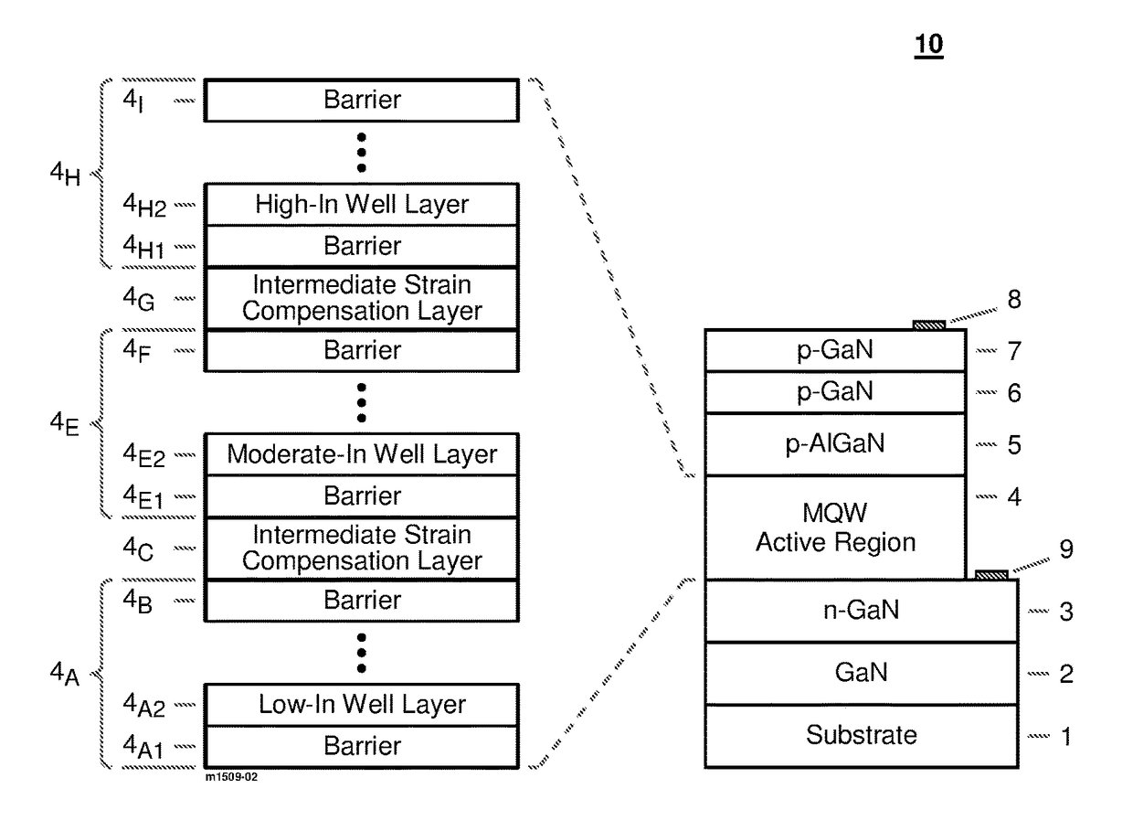
[0017]The invention relates to long wavelength light emission III-nitride based semiconductor light emitting structures, such as LEDs LDs, fabricated by means of manipulating the crystalline strain inside the light emitting active region of the structure during the epitaxial growth process. Herein and without limitation, the III-nitride semiconductor light emitter structure of this invention is illustrated within the context of an LED device structure, however a person skilled in the art will recognize how to apply the methods of this invention to the design of other III-nitride semiconductor light emitters including without limitation, LDs.

[0018]The present invention discloses an innovative method of fabricating III-nitride based light emitting structures, such as LEDs or LDs that do not suffer from excessive phase separation and thus are capable of emitting amber-to-red light with high spectral purity. Additional advantages and other features of the present invention are set forth...


PUM


Abstract

A III-nitride semiconductor light emitting device incorporating n-type III-nitride cladding layers, indium containing III-nitride light emitting region, and p-type III-nitride cladding layers. The light emitting region is sandwiched between n- and p-type III-nitride cladding layers and includes multiple sets of multi-quantum-wells (MQWs). The first MQW set formed on the n-type cladding layer comprises relatively lower indium concentration. The second MQW set comprising relatively moderate indium concentration. The third MQW set adjacent to the p-type cladding layer incorporating relatively highest indium concentration of the three MQW sets and is capable of emitting amber-to-red light. The first two MQW sets are utilized as pre-strain layers. Between the MQW sets, intermediate strain compensation layers (ISCLs) are added. The combination of the first two MQW sets and ISCLs prevent phase separation and enhance indium uptake in the third MQW set. The third MQW set, as a result, retains sufficiently high indium concentration to emit amber-to-red light of high output power without any phase separation associated problems.

Description

CROSS-REFERENCE TO RELATED APPLICATIONS[0001]This application claims the benefit of U.S. Provisional Patent Application No. 62 / 239,122 filed Oct. 8, 2015.BACKGROUND OF THE INVENTION[0002]1. Field of the Invention[0003]The invention herein relates generally to a III-nitride semiconductor light emitting device that emits visible light in the amber-to-red region. A method to manufacture the same is disclosed.[0004]2. Prior Art[0005]Prior art III-nitride based blue light emitting structures, such as light diodes (LEDs) and laser diodes (LD), (for the sake of brevity, LEDs and LDs may each be referred to as LEDs herein) are commercially available with peak external quantum efficiency (EQE) exceeding 80%. Operating in green spectral region, the EQE of prior art LEDs drops below half that of blue LEDs. The EQE of III-nitride semiconductor light emitters, very abruptly drops even more so toward the amber and red spectra region. There are two common reasons for the efficiency loss in III-nit...

Claims


Application Information

Patent Timeline
IPC IPC(8): H01L33/06H01L33/00H01L33/32
CPCH01L33/06H01L33/0075H01L33/32H01L33/02H01L33/12H01L33/30H01L33/145
Inventor YEH, YEA-CHUAN MILTONEL-GHOROURY, HUSSEIN S.LI, XINGCHEN, JYH-CHIACHUANG, CHIH-LI
Owner OSTENDO TECH INC
Why Eureka
Try Eureka