Semiconductor Device

a technology of semiconductors and devices, applied in the direction of transistors, basic electric elements, logic circuits characterised by logic functions, etc., can solve the problems of large number of transistors and low power consumption, and achieve the effect of low power consumption and small area

Inactive Publication Date: 2017-04-20
SEMICON ENERGY LAB CO LTD
View PDF10 Cites 11 Cited by
  • Summary
  • Abstract
  • Description
  • Claims
  • Application Information

AI Technical Summary

Benefits of technology

[0033]According to one embodiment of the present invention, a semiconductor device with a small number of transistors can be provided. According to one embodiment of the present invention, a semiconductor device with a small area can

Problems solved by technology

A complementary metal oxide semiconductor (CMOS) logic circuit used for a large-scale integrated (LSI) circuit has a problem in that the number

Method used


Image

  • Semiconductor Device
  • Semiconductor Device
  • Semiconductor Device

Examples


embodiment 1

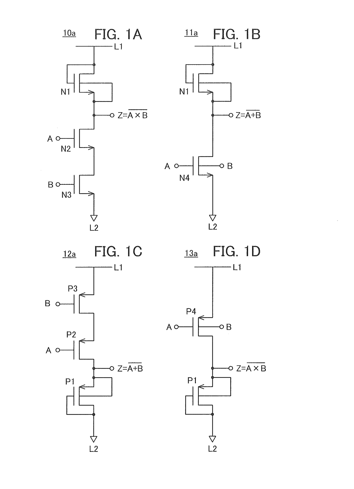
[0067]FIGS. 1A to 1D each illustrate an example of a circuit configuration of a semiconductor device of one embodiment of the present invention.

10a>>

[0068]A semiconductor device 10a illustrated in FIG. 1A includes a transistor N1, a transistor N2, a transistor N3, a wiring L1, and a wiring L2. The transistor N1, the transistor N2, and the transistor N3 are n-channel transistors. The wiring L1 and the wiring L2 are supplied with a high power supply potential (VDD) and a low power supply potential (GND), respectively.

[0069]The transistor N1 includes a first gate and a second gate. In the transistor N1, the first gate and the second gate preferably overlap with each other with a semiconductor therebetween.

[0070]The first gate of the transistor N1 is electrically connected to a first terminal of the transistor N1. The second gate of the transistor N1 is electrically connected to a second terminal of the transistor N1. The first terminal of the transistor N1 is electrically connect...

embodiment 2

[0132]In this embodiment, an OS transistor that can be used in the semiconductor device of Embodiment 1 will be described.

Structure Example 1 of Transistor

[0133]FIGS. 8A and 8B show cross-sectional views and a top view of a transistor 100a. FIG. 8B is a top view. A cross section taken along the dashed-dotted line X1-X2 in FIG. 8B is illustrated on the left side of FIG. 8A, and a cross section taken along the dashed-dotted line Y1-Y2 in FIG. 8B is illustrated on the right side of FIG. 8A. Note that for simplification of the drawings, some components are increased or reduced in size, or omitted in FIGS. 8A and 8B. The direction of the dashed-dotted line X1-X2 may be called a channel length direction, and the direction of the dashed-dotted line Y1-Y2 may be called a channel width direction.

[0134]Note that the channel length refers to, for example, a distance between a source (a source region or a source electrode) and a drain (a drain region or a drain electrode) in a region where a se...

example 3

Structure Example 3 of Transistor

[0208]FIGS. 11A and 11B show cross-sectional views and a top view of a transistor 100d. FIG. 11B is a top view. A cross section taken along the dashed-dotted line X1-X2 in FIG. 11B is illustrated on the left side of FIG. 11A, and a cross section taken along the dashed-dotted line Y1-Y2 in FIG. 11B is illustrated on the right side of FIG. 11A. Note that for simplification of the drawings, some components are increased or reduced in size, or omitted in FIGS. 11A and 11B. The direction of the dashed-dotted line X1-X2 may be called a channel length direction, and the direction of the dashed-dotted line Y1-Y2 may be called a channel width direction.

[0209]The transistor 100d is different from the transistor 100a in that a groove is provided in the insulator 106 and the semiconductor 113, the insulator 114, and the conductor 109 are positioned in the groove. The transistor 100d is preferable in that the parasitic capacitance generated between the conductor ...


PUM


Abstract

A semiconductor device with a small number of transistors is provided. The semiconductor device includes a first transistor, a second transistor, a third transistor, a first wiring, and a second wiring. The first transistor includes a first gate and a second gate. The first gate and the second gate overlap with each other with a semiconductor therebetween. The first wiring and the second wiring are supplied with a high power supply potential and a low power supply potential, respectively. A first terminal of the first transistor is electrically connected to the first gate and the first wiring. A second terminal of the first transistor is electrically connected to the second gate. The second terminal of the first transistor is electrically connected to the second wiring through the second transistor and the third transistor. The first transistor, the second transistor, and the third transistor are preferably n-channel transistors.

Description

BACKGROUND OF THE INVENTION[0001]1. Field of the Invention[0002]One embodiment of the present invention relates to a semiconductor device.[0003]The present invention relates to an object, a method, or a manufacturing method. In addition, the present invention relates to a process, a machine, manufacture, or a composition of matter.[0004]In this specification and the like, a semiconductor device generally means a device that can function by utilizing semiconductor characteristics. In some cases, a memory device, a display device, a light-emitting device, an electro-optical device, a semiconductor circuit, or an electronic device includes a semiconductor device.[0005]2. Description of the Related Art[0006]A complementary metal oxide semiconductor (CMOS) logic circuit used for a large-scale integrated (LSI) circuit has a problem in that the number of transistors is large. In contrast, in the case of a pass transistor logic circuit, a complicated logic can be formed with a small number ...

Claims


Application Information

Patent Timeline
IPC IPC(8): H01L27/088H01L23/535H01L27/115H01L29/24
CPCH01L27/088H01L27/115H01L23/535H01L29/24H03K19/0027H03K19/20H01L29/78648H01L29/78696H01L27/1225H01L27/0826H01L21/8238H01L27/092H01L29/517H10B69/00
Inventor IKEDA, TAKAYUKI
Owner SEMICON ENERGY LAB CO LTD
Why Eureka
Try Eureka