

Semiconductor Structure with Stress-Reducing Buffer Structure
- Summary
- Abstract
- Description
- Claims
- Application Information
AI Technical Summary
Benefits of technology
Problems solved by technology
Method used
Image

Examples
Embodiment Construction
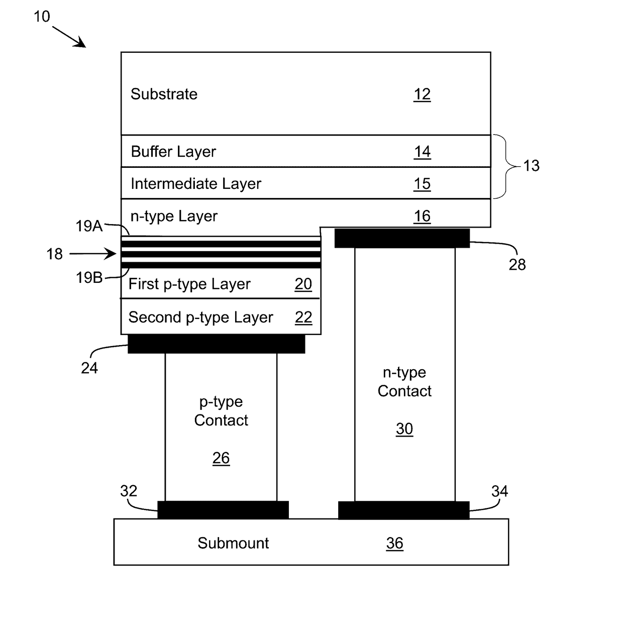
[0030]As indicated above, aspects of the invention provide a semiconductor structure comprising a buffer structure and a set of semiconductor layers formed adjacent to a first side of the buffer structure. The buffer structure can have an effective lattice constant and a thickness such that an overall stress in the set of semiconductor layers at room temperature is compressive and is in a range between approximately 0.1 GPa and 2.0 GPa. The buffer structure can be grown using a set of growth parameters selected to achieve the target effective lattice constant a, control stresses present during growth of the buffer structure, and / or control stresses present after the semiconductor structure has cooled.
[0031]As described herein, the buffer structure can be configured to reduce internal stresses in the heterostructure, which can lead to improved reliability of the device. The buffer structure, as well as other layers of the heterostructure, can be grown using growth parameters configur...
PUM
 Abstract
Description
Claims
Application Information