Nitride semiconductor device

a technology of semiconductor devices and nitride, which is applied in the direction of semiconductor devices, electrical devices, transistors, etc., can solve the problems of not increasing the speed of switching, and achieve the effect of reducing resistan

Inactive Publication Date: 2017-05-11
PANASONIC INTELLECTUAL PROPERTY MANAGEMENT CO LTD
View PDF18 Cites 17 Cited by
  • Summary
  • Abstract
  • Description
  • Claims
  • Application Information

AI Technical Summary

Benefits of technology

[0032]The nitride semiconductor device according to the present disclosure can reduce the resistance at the contact between the p-type nitride semiconductor layer and the metal line layer. Thus, the present disclosure provides a power switching nitride semiconductor device capable of high-speed switching.

Problems solved by technology

However, such conventional nitride semiconductor devices that establish contact by arranging precious metals such as Ti and Pt on the p-type nitride semiconductor layer will not be able to sufficiently reduce the resistance at the contact between the p-type nitride semiconductor layer and the metal line layer and therefore cannot increase the speed of switching.

Method used


Image

  • Nitride semiconductor device
  • Nitride semiconductor device
  • Nitride semiconductor device

Examples


embodiment 1

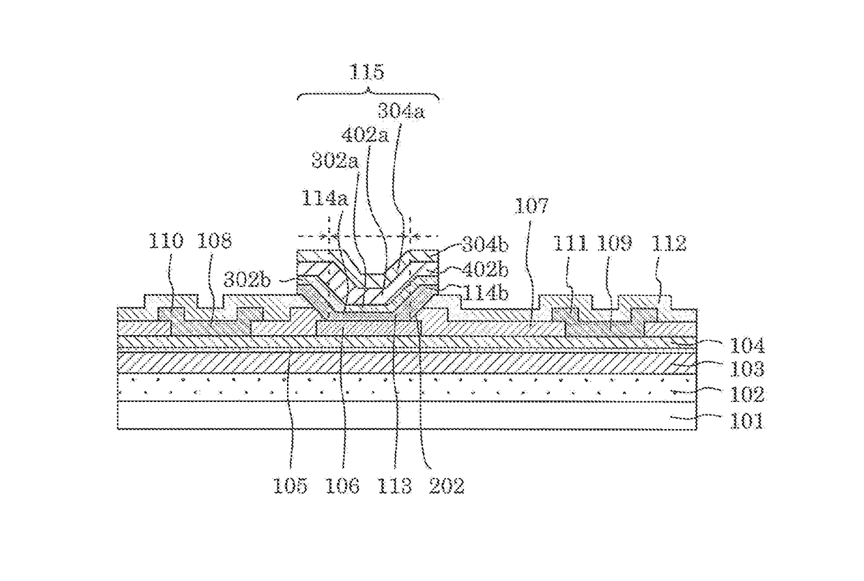
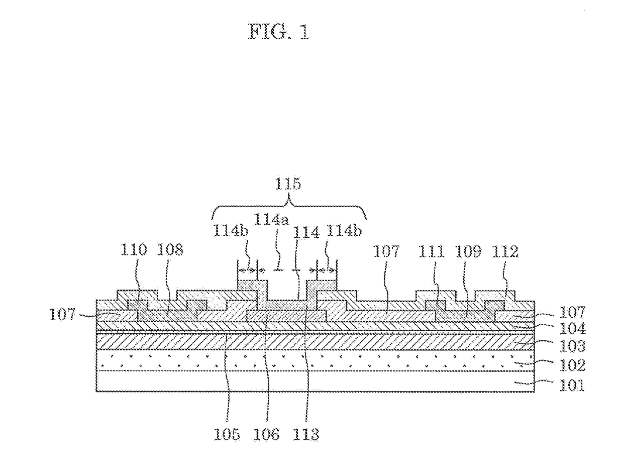
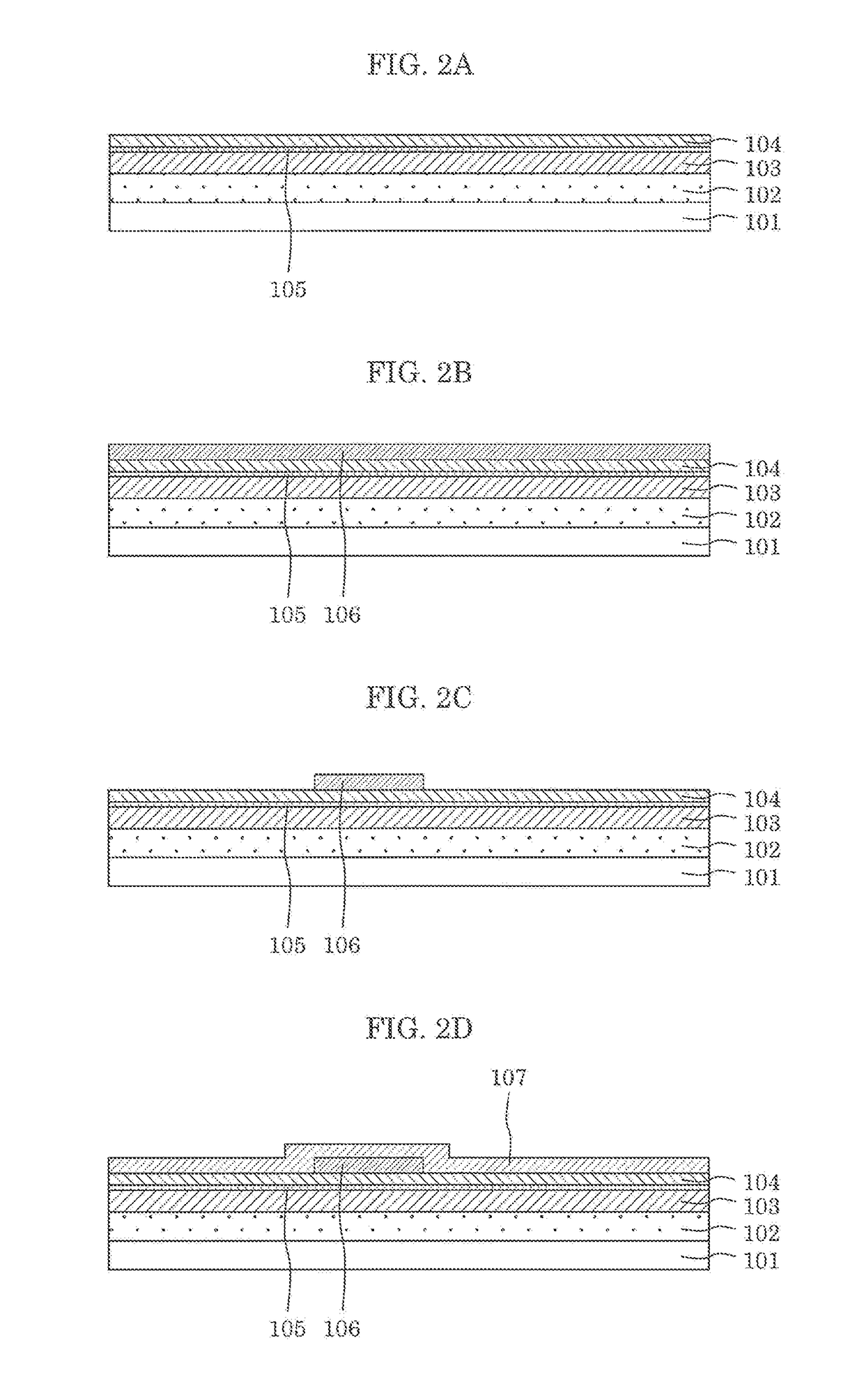
[0105]FIG. 1 is a cross-sectional view of a nitride semiconductor device according to Embodiment 1 of the present disclosure. As illustrated in FIG. 1, the nitride semiconductor device according to the present embodiment includes, for example, substrate 101 made of silicon (Si), buffer layer 102 having a thickness of 2 μm and a stacked structure of a plurality of layers including aluminum nitride (AlN) and aluminum gallium nitride (AlGaN), undoped (i-type) GaN layer 103 having a thickness of 2 μm, and i-type AlGaN layer 104 having a thickness of 25 nm and an aluminum (Al) composition ratio of 15%, in such a manner that buffer layer 102, i-type GaN layer 103, and i-type AlGaN layer 104 are formed on substrate 101. Two dimensional electron gas 105 is generated at the heterointerface between i-type AlGaN layer 104 and i-type GaN layer 103. The term “undoped (i-type)” as used herein means that the layer is not intentionally doped with impurities during epitaxial growth.

[0106]The nitride...

embodiment 2

[0165]FIG. 14 is a cross-sectional view of a nitride semiconductor device according to Embodiment 2. As illustrated in FIG. 14, the nitride semiconductor device according to the present embodiment includes, for example, substrate 101 made of Si, buffer layer 102 having a thickness of 2 μm and having a stacked structure of a plurality of layers including AlN and AlGaN, undoped (i-type) GaN layer 103 having a thickness of 2 μm, and i-type AlGaN layer 104 having a thickness of 25 nm and an Al composition ratio of 15%, in such a manner that buffer layer 102, i-type GaN layer 103, and i-type AlGaN layer 104 are formed on substrate 101. Two dimensional electron gas 105 is generated at the heterointerface between i-type AlGaN layer 104 and i-type GaN layer 103. The nitride semiconductor device according to the present embodiment also includes p-type GaN layer 106 having a thickness of 200 nm and being processed in a predetermined shape on the surface of i-type AlGaN layer 104. Here, p-type...

embodiment 3

[0204]FIG. 24 is a cross-sectional view of a nitride semiconductor device according to Embodiment 3. As illustrated in FIG. 24, the nitride semiconductor device according to the present embodiment includes, for example, substrate 101 made of Si, buffer layer 102 having a thickness of 2 μm and a stacked structure of a plurality of layers including AlN and AlGaN, undoped (i-type) GaN layer 103 having a thickness of 2 μm, and i-type AlGaN layer 104 having a thickness of 25 nm and an Al composition ratio of 15%, in such a manner that buffer layer 102, i-type GaN layer 103, and i-type AlGaN layer 104 are formed on substrate 101. Two dimensional electron gas 105 is generated at the heterointerface between i-type AlGaN layer 104 and i-type GaN layer 103. The nitride semiconductor device according to the present embodiment also includes p-type GaN layer 106 having a thickness of 200 nm and being processed in a predetermined shape on the surface of i-type AlGaN layer 104. Here, p-type GaN la...


PUM

PropertyMeasurementUnit
thicknessaaaaaaaaaa
thicknessaaaaaaaaaa
total thicknessaaaaaaaaaa

Abstract

A nitride semiconductor device according to the present disclosure includes a substrate, a p-type GaN layer formed on a main surface of the substrate and made of AlxInyGa1-x-yN containing p-type impurities, where 0≦X<1, 0≦Y<1, and a Ti film formed on the p-type GaN layer. The Ti film is in a coherent or metamorphic state with respect to the p-type GaN layer.

Description

CROSS REFERENCE TO RELATED APPLICATIONS[0001]This application is a U.S. continuation application of PCT International Patent Application Number PCT / JP2015 / 003709 filed on Jul. 24, 2015, claiming the benefit of priority of Japanese Patent Application Number 2014-153514 filed on Jul. 29, 2014, the entire contents of which are hereby incorporated by reference.BACKGROUND[0002]1. Technical Field[0003]The present disclosure relates to a nitride semiconductor device using a p-type nitride semiconductor.[0004]2. Description of the Related Art[0005]Power switching field effect transistors (FETs) need to achieve low on-state resistance in order to reduce power loss. Additionally, the interruption of current flow at zero bias, i.e., normally off characteristics, are dispensable from the viewpoint of safety.[0006]One example of technology that achieves low on-state resistance and normally off characteristics of FETs using gallium nitride (GaN) is using a p-type nitride semiconductor layer as a ...

Claims


Application Information

Patent Timeline
Patent Type & Authority Applications(United States)
IPC IPC(8): H01L29/778H01L29/808H01L29/20H01L29/04H01L21/283H01L29/66H01L27/098H01L29/812
CPCH01L29/7787H01L27/098H01L29/808H01L29/2003H01L29/045H01L21/283H01L29/66462H01L29/812H01L21/28H01L29/452H01L29/7786H01L29/1066
Inventor ETOU, RYUUJIHARADA, TAKESHIHAMADA, MASAKAZUSHIBATA, TAMOTSU
Owner PANASONIC INTELLECTUAL PROPERTY MANAGEMENT CO LTD
Why Eureka
Try Eureka