Touch panels and the driving method thereof

a technology of touch panel and driving method, which is applied in the direction of electric digital data processing, instruments, computing, etc., can solve the problems of increasing the number of cog pins and the manufacturing difficulties of bonding, affecting display performance and touch sensibility, and increasing the coupling capacitance between the two wirings. , to achieve the effect of reducing the number of pins, reducing the difficulty of bonding manufacturing process, and reducing the coupling capacitance between the wirings

Active Publication Date: 2017-05-18
TCL CHINA STAR OPTOELECTRONICS TECH CO LTD +1
View PDF25 Cites 10 Cited by
  • Summary
  • Abstract
  • Description
  • Claims
  • Application Information

AI Technical Summary

Benefits of technology

[0007]The object of the invention is to provide a touch panel and the driving method thereof for reducing the difficulties in bonding manufacturing process. In this way, the display performance and the touch sensibility are improved.
[0023]In view of the above, at least a portion of the pins of the driving chip is configured to provide the first driving signals and the second driving signals in a time-sharing manner. This not only reduces the number of the pins within the driving chip, but also reduces the difficulties of the bonding manufacturing process. At the same time, the number of wirings within the fan area corresponding to the pins is reduced, such that the wirings are not overlapped by each other. In this way, the coupling capacitance between the wirings is reduced, and thus the display performance and the touch sensibility of the touch panel are enhanced.

Problems solved by technology

This design increases the number of COG pins and the manufacturing difficulties of bonding.
In addition, the touch wiring and the LCD wiring of the COG output may greatly overlap in the fan-out area, which may increase the coupling capacitance between the two wirings such that the display performance and the sensibility of the touch are affected.

Method used


Image

  • Touch panels and the driving method thereof
  • Touch panels and the driving method thereof
  • Touch panels and the driving method thereof

Examples


Embodiment Construction

[0031]Embodiments of the invention will now be described more fully hereinafter with reference to the accompanying drawings, in which embodiments of the invention are shown.

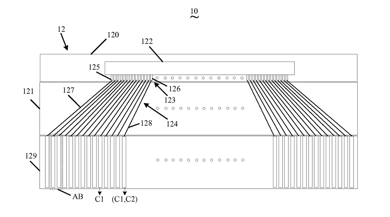
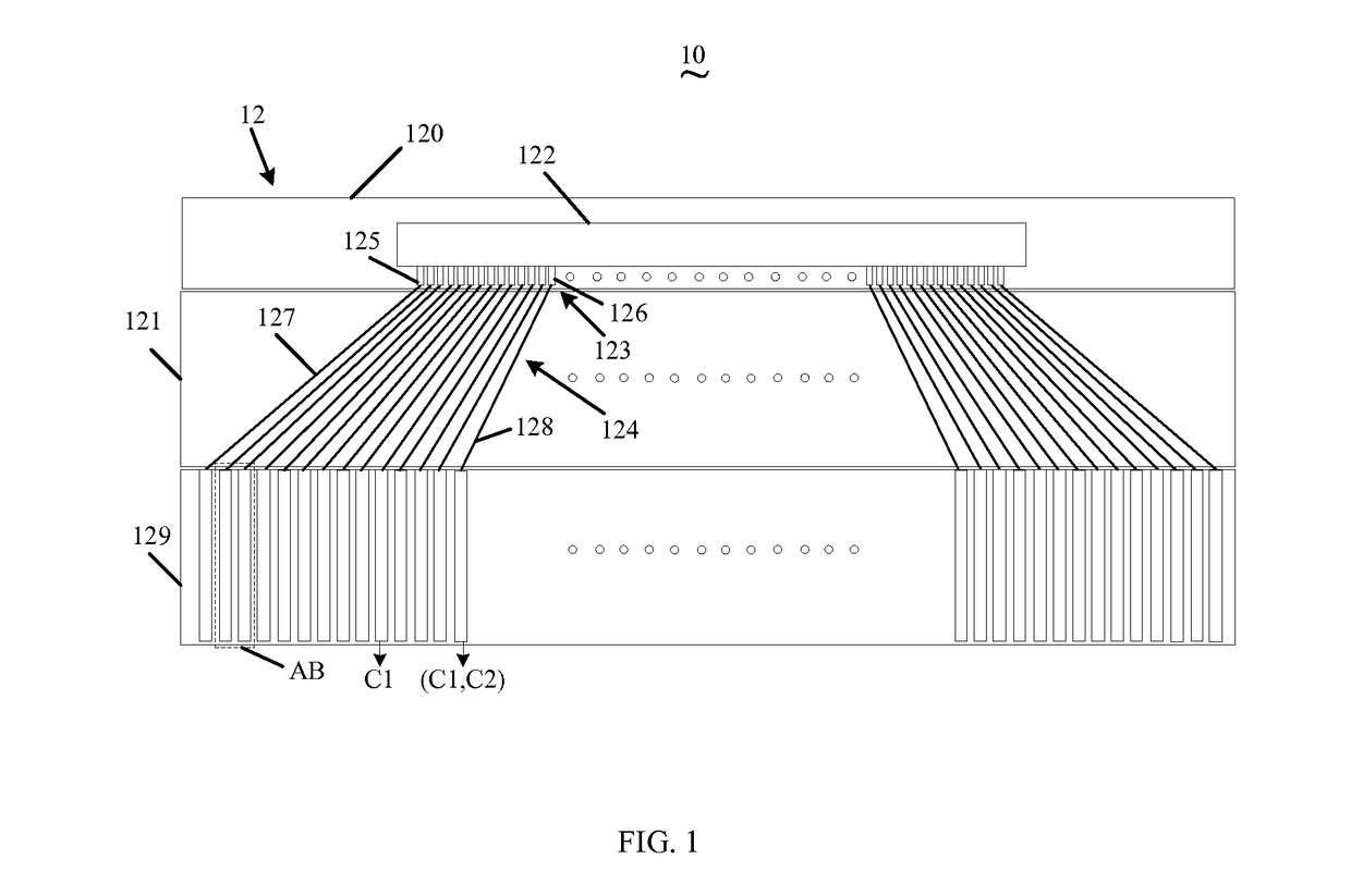
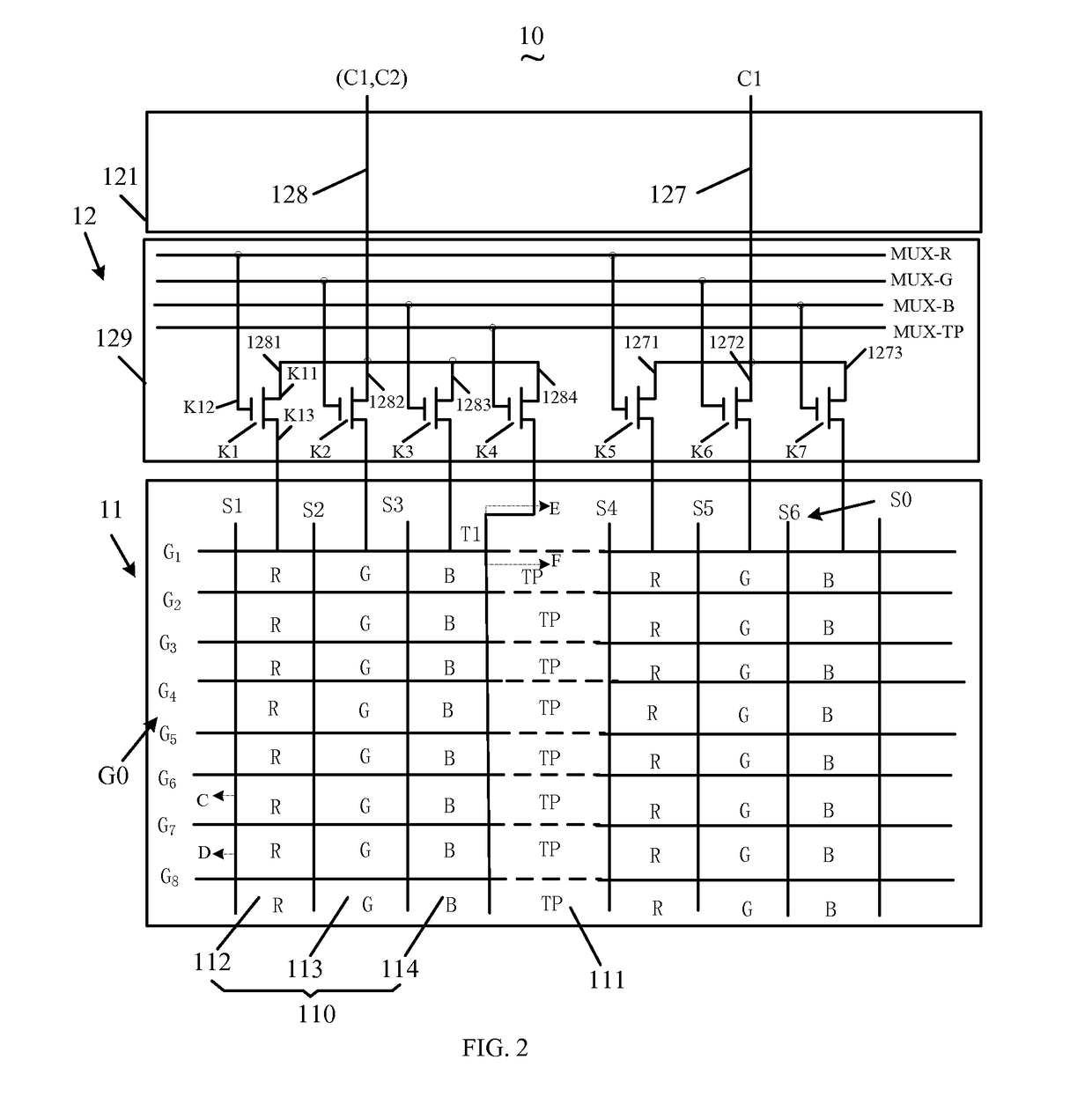
[0032]Referring to FIGS. 1 and 2, FIG. 1 is a schematic view showing the partial touch panel in accordance with one embodiment, and FIG. 2 is a schematic view showing the partial touch panel in accordance with another embodiment. As shown in FIGS. 1 and 2, the touch panel 10 includes a display area 11 and a non-display area 12.

[0033]The display area 11 includes a plurality of pixel electrodes 110 and touch sensors 111. The display area 11 includes a plurality of scanning lines (G0), data lines (S0), and a touch-driving-signals line (T1). To simply the descriptions, there are only eight scanning lines (G1-G8), six data lines (S1-S6) and one touch-driving-signals line (T1) are shown in this embodiment. It can be understood that the present disclosure is not limited to the above example. Each of the pixel electrodes...


PUM

PropertyMeasurementUnit
areaaaaaaaaaaa
gap densityaaaaaaaaaa
voltageaaaaaaaaaa

Abstract

A touch panel and a driving method are described in the present disclosure. A driving chip is arranged within a chip area of a non-display area. The driving chip includes a plurality of pins. At least a portion of the pins outputs first driving signals for controlling the pixel electrodes, and outputs second driving signals for controlling the touch sensor. A plurality of wirings corresponding to the pins is arranged within the fan area, and the wirings transmit the first driving signals and the second driving signals outputted by the pins. In view of the above, the difficulties of the bonding manufacturing process are reduced. At the same time, the coupling capacitance between the wirings is reduced, and thus the display performance and the touch sensibility of the touch panel 10 are enhanced.

Description

BACKGROUND OF THE INVENTION[0001]1. Field of the Invention[0002]The present disclosure relates to liquid crystal display technology, and more particularly to a touch panel and the driving method thereof.[0003]2. Discussion of the Related Art[0004]Liquid crystal displays (LCDs) are the most popular display devices been widely adopted by mobile phones, personal digital assistants (PDAs), digital cameras, and computers. With the development of the liquid crystal technology, consumers demand toward higher performance and better design, such as low cost and narrow border.[0005]Touch technology has been greatly developed in recent years. A variety of touch technologies have been adopted during mass production. In-cell touch is one of the popular touch technology due to its integration and low cost. Conventional, two independent integrated circuit (IC) are configured, wherein one relates to in-cell touch, and the other one relates to driving the LCD. With the technology development, touch ...

Claims


Application Information

Patent Timeline
Patent Type & Authority Applications(United States)
IPC IPC(8): G06F3/041G02F1/1345G02F1/1343G02F1/1362G06F3/044G02F1/1333
CPCG06F3/0418G06F3/044G06F3/0412G02F1/13338G02F1/134309G02F2001/134345G02F1/13452G02F1/133345G06F2203/04103G06F2203/04111G02F1/136286G09G3/3611G09G3/3688G09G2310/0297G09G2354/00G02F1/13454G06F3/04164G06F3/04184G02F1/134345G09G3/3685
Inventor HAO, SIKUN
Owner TCL CHINA STAR OPTOELECTRONICS TECH CO LTD
Why Eureka
Try Eureka