Nitride compound semiconductor

Active Publication Date: 2017-05-18
ROHM CO LTD
View PDF3 Cites 0 Cited by
  • Summary
  • Abstract
  • Description
  • Claims
  • Application Information

AI Technical Summary

Benefits of technology

The present invention provides a nitride compound semiconductor with improved heat dissipation. This is achieved by introducing a recess where a heat dissipation layer and a layer with higher thermal conductivity are placed. This allows for better heat dissipation from the semiconductor, improving its reliability for use in semiconductor electron devices.

Problems solved by technology

After the growth of the nitride compound semiconductor stack, the Si substrate not only becomes convex downward but can also crack because of the stress in the crystal itself.

Method used


Image

  • Nitride compound semiconductor
  • Nitride compound semiconductor
  • Nitride compound semiconductor

Examples


embodiment 1

[0027]A nitride compound semiconductor according to Embodiment 1 of the present invention includes, as illustrated in FIG. 1, a substrate 1 and a nitride compound semiconductor stack 11 on this substrate 1. The nitride compound semiconductor can be, for example, an epitaxial wafer.

[0028]The substrate 1 is, for example, a 0.01-Ω·cm boron-doped CZ Si substrate. The substrate 1 can be any substrate on which a nitride compound semiconductor can be epitaxially grown. Examples include Si, SiC, GaN and sapphire substrates.

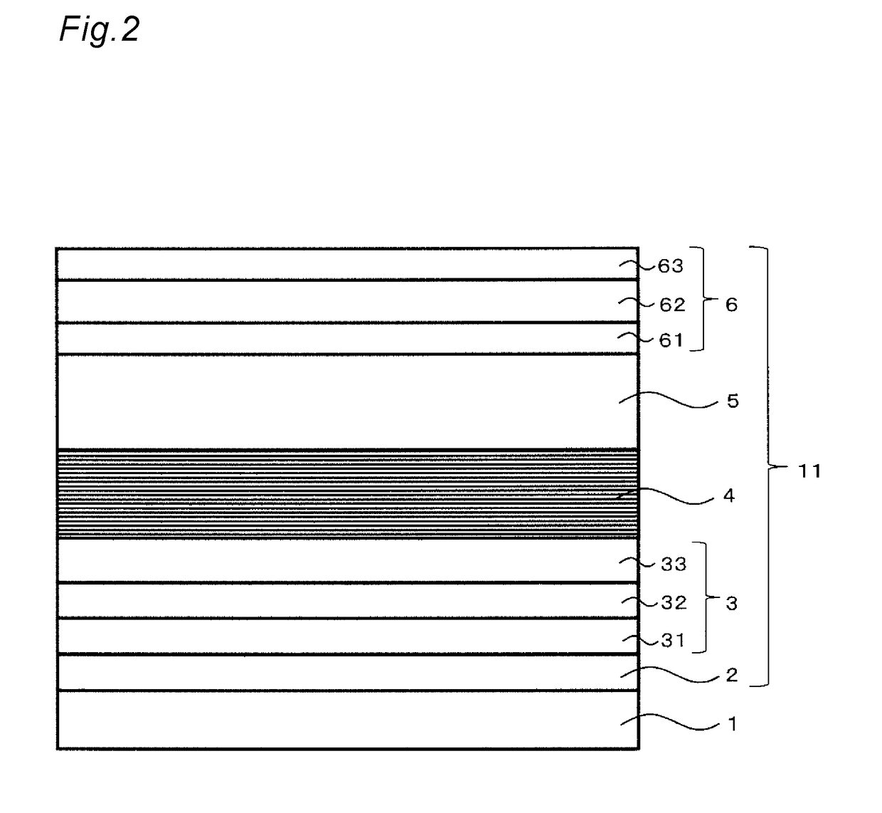
[0029]The nitride compound semiconductor stack 11 consists of an initial growth layer 2, a composition-gradient buffer layer 3, a multilayer buffer layer 4, a GaN channel layer 5, and an electron supply layer 6 and has a structure in which the initial growth layer 2, the composition-gradient buffer layer 3, the multilayer buffer layer 4, the GaN channel layer 5, and the electron supply layer 6 are stacked in order.

[0030]The initial growth layer 2 is, for example, a 100-nm...

embodiment 2

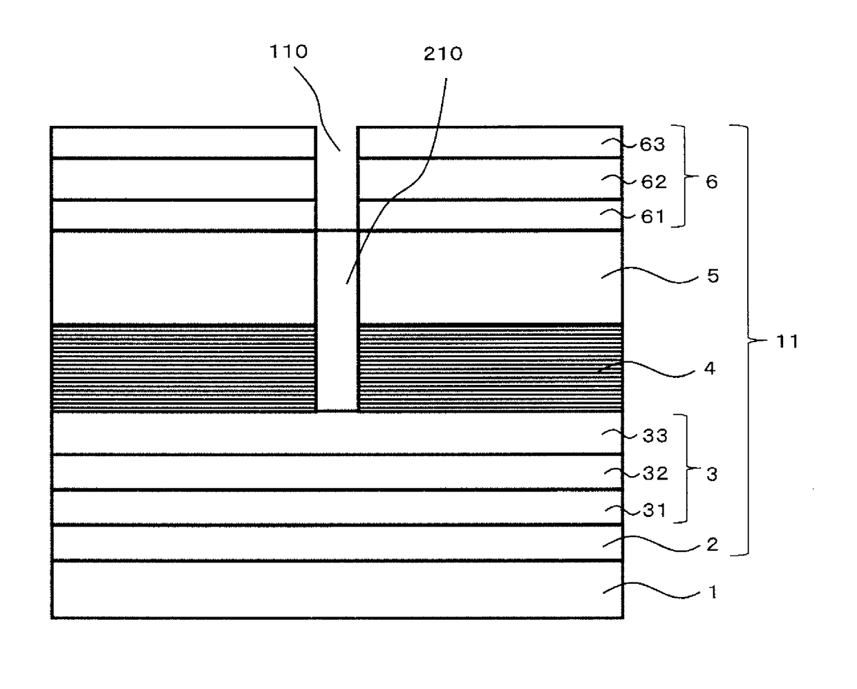
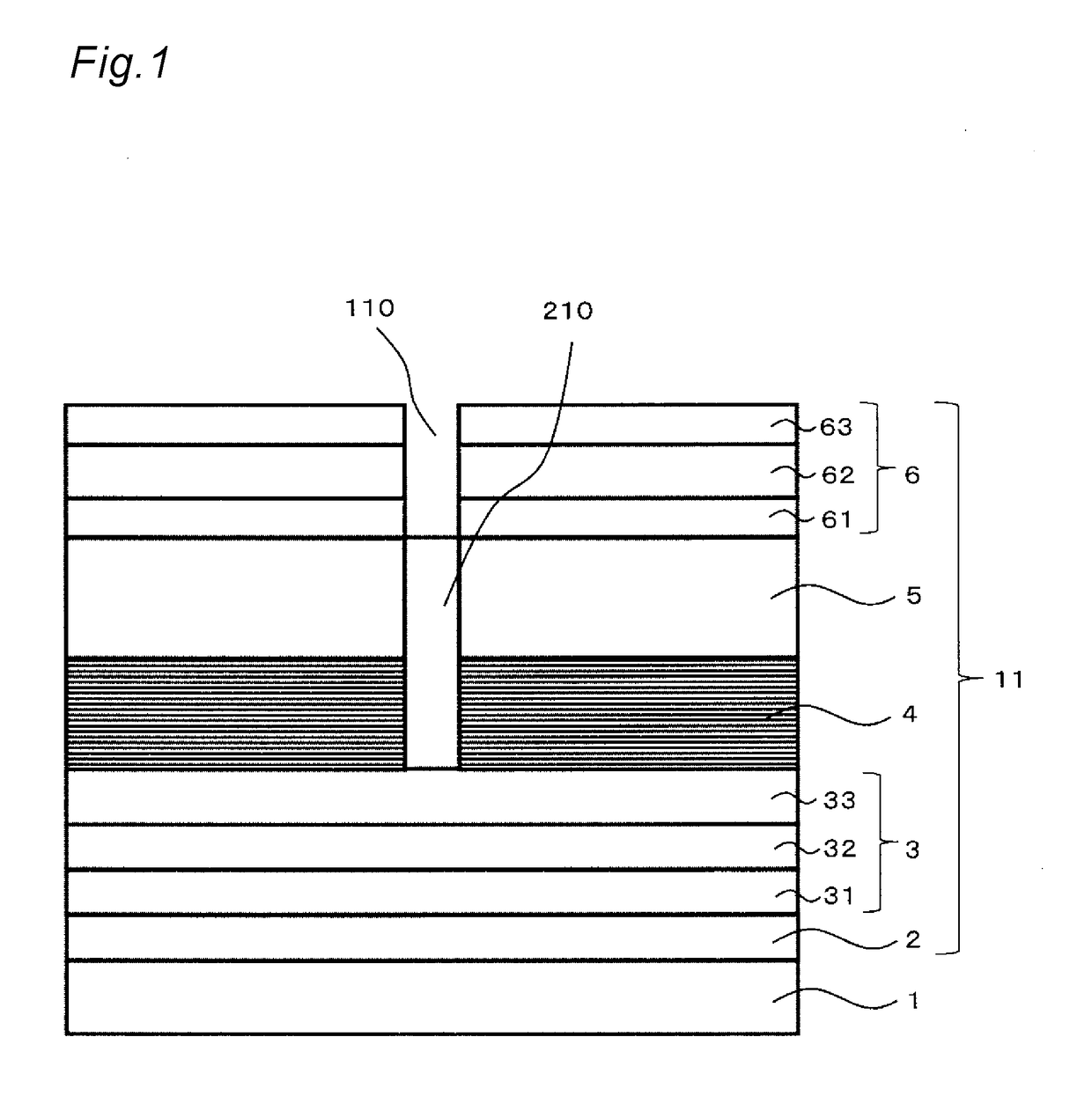
[0052]A nitride compound semiconductor according to Embodiment 2 has, as illustrated in FIG. 4, a recess 120 in the nitride compound semiconductor stack 11 according to Embodiment 1 that extends from the surface of the electron supply layer 6 to the initial growth layer 2 through the electron supply layer 6, the GaN channel layer 5, the multilayer buffer layer 4, and the composition-gradient buffer layer 3, with a GaN heat dissipation layer 220 in this recess 120. The structural portions identical to those in Embodiment 1 above are given the same numerals as in Embodiment 1. To these structural portions, the descriptions in Embodiment 1 apply.

[0053]Besides being contiguous to the GaN channel layer 5, the multilayer buffer layer 4, and the composition-gradient buffer layer 3, the heat dissipation layer 220 prevents the GaN channel layer 5, the multilayer buffer layer 4, and the composition-gradient buffer layer 3 from being exposed in the recess 120. This recess 120 is in a portion (...

embodiment 3

[0056]A nitride compound semiconductor according to Embodiment 3 includes, as illustrated in FIG. 5, a substrate 1 and a nitride compound semiconductor stack 13 on this substrate 1. The nitride compound semiconductor stack 13 consists of an initial growth layer 2, a multilayer buffer layer 4, a GaN channel layer 5, and an electron supply layer 106 and has a structure in which the initial growth layer 2, the multilayer buffer layer 4, the GaN channel layer 5, and the electron supply layer 106 are stacked in order. The structural portions identical to those in Embodiments 1 and 2 above are given the same numerals as in Embodiments 1 and 2. To these structural portions, the descriptions in Embodiments 1 and 2 apply.

[0057]The electron supply layer 106 is, for example, a 25-nm thick Al0.22Ga0.78N barrier layer. In Embodiment 3, the thickness of the initial growth layer 2 is 120 nm, the multilayer buffer layer 4 is a stack in which an AlN layer (5 nm thick) / Al0.1Ga0.9N layer (30 nm thick)...


PUM


Abstract

A nitride compound semiconductor has a substrate and a nitride compound semiconductor stack on the substrate. The nitride compound semiconductor stack includes a multilayer buffer layer, a channel layer on this multilayer buffer layer, and an electron supply layer on this channel layer. A recess extends from the surface of the electron supply layer through the channel layer and the multilayer buffer layer. A heat dissipation layer in this recess is contiguous to the multilayer buffer layer and the channel layer and has a higher thermal conductivity than the multilayer buffer layer.

Description

TECHNICAL FIELD[0001]The present invention relates to a nitride compound semiconductor.BACKGROUND ART[0002]A typical known nitride compound semiconductor for semiconductor electronic devices is a nitride compound semiconductor having an AlGaN—GaN heterojunction. This nitride compound semiconductor unit is composed of, for example, a substrate, a nitride compound semiconductor stack on the substrate, source and drain electrodes, and a gate electrode between the source and drain electrodes. The substrate is a sapphire, Si, or similar substrate. The semiconductor stack is composed of a buffer layer, a channel layer typically made of GaN, and an AlGaN barrier layer. The source and drain electrodes make ohmic contacts with a two-dimensional electron gas formed at the interface between the barrier and channel layers.[0003]In fabricating this known nitride compound semiconductor, it is not a very big problem if the nitride compound semiconductor stack is formed on a sapphire or SiC substra...

Claims


Application Information

Patent Timeline
IPC IPC(8): H01L29/06H01L29/812H01L29/66H01L29/205H01L29/10H01L23/373H01L29/778H01L29/20
CPCH01L29/0634H01L29/7787H01L29/812H01L29/66462H01L29/205H01L29/1054H01L23/3738H01L29/2003H01L23/3677H01L29/7786H01L29/0657
Inventor ITO, NOBUYUKITOHSAKI, MANABUOGAWA, ATSUSHI
Owner ROHM CO LTD
Why Eureka
Try Eureka