Wafer producing method

a production method and technology of wafers, applied in the direction of manufacturing tools, polycrystalline material growth, after-treatment details, etc., can solve the problems of poor economy, poor economy, poor economy, etc., and achieve the effect of improving economy and good economy

Active Publication Date: 2017-06-01
DISCO CORP
View PDF62 Cites 26 Cited by
  • Summary
  • Abstract
  • Description
  • Claims
  • Application Information

AI Technical Summary

Benefits of technology

[0015]According to the wafer producing method of the present invention, it is unnecessary to process a hexagonal single crystal ingot obtained by crystal growth into a cylindrical shape so that the side surface of the ingot processed is inclined by 3.5°, 4.0°, or 8.0° with respect to the c-axis. Accordingly, no waste is generated from the hexagonal single crystal ingot, thereby achieving good economy. Further, the laser beam is applied to the ingot to thereby form the modified layers inside the i

Problems solved by technology

However, when the ingot is cut by the wire saw and both sides of each wafer are polished to obtain the product, 70% to 80% of the ingot is discarded to cause a problem of poor economy.
In particular, a hexagonal single crystal ingot of SiC or GaN, for example, has high Mohs hardness and it is therefore difficult to cut this ingot with the wire saw, causing a reduction in productivity.
Further, when a hexagonal single crystal ingot having a c-plane on the upper surface thereof as manufactured by crystal growth is processed to obtain a cylindrical hexa

Method used


Image

  • Wafer producing method
  • Wafer producing method
  • Wafer producing method

Examples


Embodiment Construction

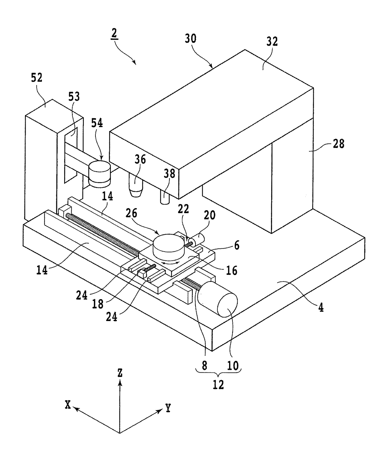
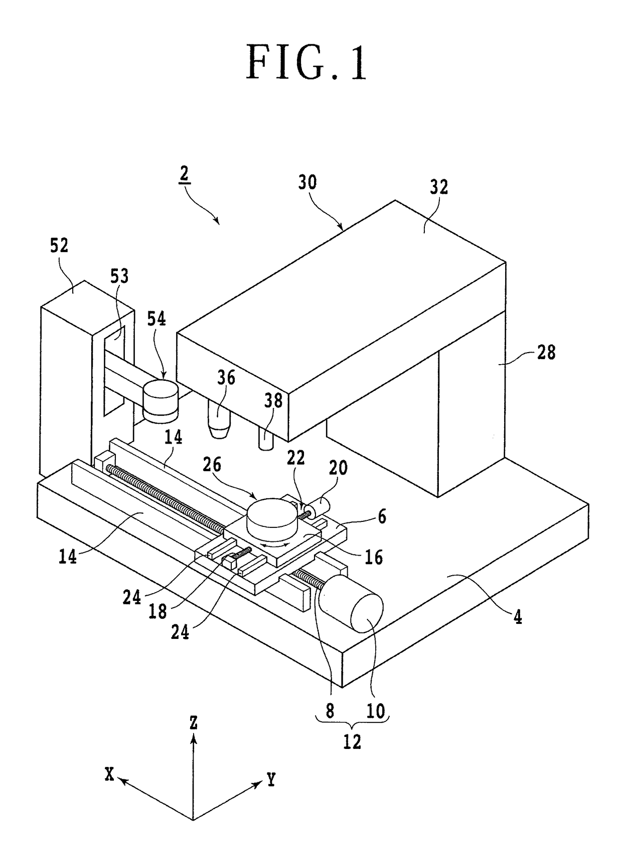
[0036]Preferred embodiments of the present invention will now be described in detail with reference to the drawings. Referring to FIG. 1, there is shown a perspective view of a laser processing apparatus 2 suitable for use in performing the wafer producing method of the present invention. The laser processing apparatus 2 includes a stationary base 4 and a first slide block 6 mounted on the stationary base 4 so as to be movable in the X direction. The first slide block 6 is moved in a feeding direction, or in the X direction along a pair of guide rails 14 by a feeding mechanism 12 composed of a ball screw 8 and a pulse motor 10.

[0037]A second slide block 16 is mounted on the first slide block 6 so as to be movable in the Y direction. The second slide block 16 is moved in an indexing direction, or in the Y direction along a pair of guide rails 24 by an indexing mechanism 22 composed of a ball screw 18 and a pulse motor 20. A support table 26 is mounted on the second slide block 16. Th...


PUM

PropertyMeasurementUnit
Lengthaaaaaaaaaa
Angleaaaaaaaaaa
Depthaaaaaaaaaa

Abstract

A wafer having an off angle α is produced from a hexagonal single crystal ingot having an upper surface, a c-plane exposed to the upper surface, and a c-axis perpendicular to the c-plane. The ingot is supported by a wedge member having a wedge angle α equal to the off angle α, thereby inclining the upper surface of the ingot by the off angle α with respect to a horizontal plane. A modified layer is formed by setting the focal point of a laser beam inside the ingot and next applying it to the upper surface, thereby linearly forming a modified layer inside the ingot and cracks extending from the modified layer along the c-plane. The focal point is moved in the second direction to index the focal point by a predetermined amount.

Description

BACKGROUND OF THE INVENTION[0001]Field of the Invention[0002]The present invention relates to a wafer producing method for slicing a hexagonal single crystal ingot to produce a wafer.[0003]Description of the Related Art[0004]Various devices such as ICs and LSIs are formed by forming a functional layer on the front side of a wafer formed of silicon or the like and partitioning this functional layer into a plurality of regions along a plurality of crossing division lines. The division lines of the wafer are processed by a processing apparatus such as a cutting apparatus and a laser processing apparatus to thereby divide the wafer into a plurality of individual device chips respectively corresponding to the devices. The device chips thus obtained are widely used in various electronic equipment such as mobile phones and personal computers. Further, power devices or optical devices such as LEDs and LDs are formed by forming a functional layer on the front side of a wafer formed of a hexa...

Claims


Application Information

Patent Timeline
IPC IPC(8): B23K26/00B23K26/53B24B7/22B28D5/00
CPCB23K26/0057B28D5/0011B23K2203/56B23K26/0006B24B7/228B23K26/53B28D5/0082B28D5/04C30B29/36C30B29/406C30B33/06B23K2103/56H01L21/02002H01L21/02598H01L21/268H01L21/76H01L21/7806H01L2924/35121
Inventor HIRATA, KAZUYA
Owner DISCO CORP
Why Eureka
Try Eureka