

Method of providing protective cavity and integrated passive components in wafer level chip scale package using a carrier wafer
a chip scale and carrier wafer technology, applied in semiconductor devices, semiconductor/solid-state device details, electrical apparatus, etc., can solve the problems of difficult handling of substrates during the fabrication of mems devices and typical fragile piezoelectric substrates
- Summary
- Abstract
- Description
- Claims
- Application Information
AI Technical Summary
Benefits of technology
Problems solved by technology
Method used
Image

Examples
Embodiment Construction
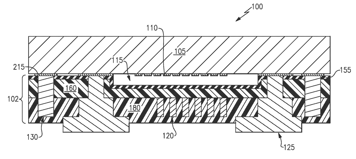
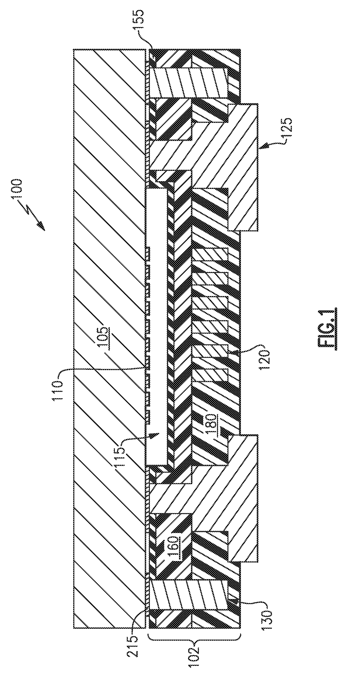
[0059]An example of a chip-scale package including a packaged SAW filter is illustrated in FIG. 1, indicated generally at 100. The SAW filter includes a piezoelectric substrate 105, for example, a lithium tantalate substrate or a sapphire substrate. Interdigital transducer (IDT) electrodes 110 of the SAW filter are disposed on the substrate 105 within a cavity 115 defined in the package 100. In some embodiments, one or more passive devices 120, for example, inductors or capacitors are disposed within material forming the body 102 of the package 100. Electrical contact bumps 125 provide electrical connection to the SAW filter IDT electrodes 110 and / or the one or more passive devices 120. The package 100 may be mounted on a printed circuit board or other substrate and the SAW filter may electrically communicate with other devices on the circuit board or other substrate through the contact bumps 125. A ring seal 130 is bonded to the substrate 105 around the IDT electrodes 110 and herme...
PUM
 Abstract
Description
Claims
Application Information