Preparation process of ceramic-based circuit board and product

A preparation process and circuit board technology, which is applied in the direction of printed circuit manufacturing, printed circuit, and printed circuit precursor manufacturing, can solve the problems of limited wire width-to-depth ratio, low thermal conductivity of finished products, and expensive preparation costs, etc., to achieve low stress, The effects of compact grains and high peel strength

Pending Publication Date: 2022-05-13
青州云领电子科技有限公司
View PDF0 Cites 0 Cited by
  • Summary
  • Abstract
  • Description
  • Claims
  • Application Information

AI Technical Summary

Problems solved by technology

The preparation method of HTCC (high temperature co-firing) requires a temperature above 1300°C, but due to the influence of electrode selection, the preparation cost is quite expensive; the preparation of LTCC (low temperature co-firing) requires a calcination process of about 850°C, but the accuracy of the prepared circuit is poor , the thermal conductivity of the finished product is low; the preparation method of DBC requires the formation of an alloy between copper foil and ceramics, and the calcination temperature needs to be strictly controlled within the temperature range of 1065-1085°C. Since the preparation method of DBC has requirements for the thickness of copper foil, generally it cannot be lower Therefore, the width-to-depth ratio of such ceramic circuit boards is limited; the preparation method of DPC includes vacuum coating, wet coating, exposure development and etching and other process links, so the price of its products is relatively high

Method used


Image

  • Preparation process of ceramic-based circuit board and product
  • Preparation process of ceramic-based circuit board and product
  • Preparation process of ceramic-based circuit board and product

Examples


preparation example Construction

[0023] A preparation process for a ceramic-based circuit board, comprising the following steps:

[0024] Vacuum plasma magnetron sputtering Cu on the surface of copper sheet 2 O, forming a layer of Cu 2 O film;

[0025] The ceramic substrate is placed on the copper sheet, and the stepwise intermittent heating method is used for bonding to obtain the circuit substrate;

[0026] Then, the stepwise intermittent cooling method is used to cool the circuit substrate;

[0027] The copper surface of the circuit substrate is recrystallized by high and low temperature alternating method, and the ceramic base circuit board is obtained by cooling.

[0028] The present invention adopts a stepwise intermittent heating method and a stepwise intermittent cooling method for continuous dynamic bonding, which can maximize the release of the stress when the copper sheet is combined with the ceramic, thereby eliminating the stress caused by the different expansion coefficients of the two materi...

Embodiment 1

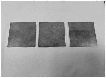
[0039] A ceramic-based circuit board, the preparation process of which is:

[0040] The OFC oxygen-free copper sheet with a size of 180mm×218mm and a thickness of 100μm was firstly cleaned with pure water and then dried, and then the two sides of the copper sheet were plated with Cu by vacuum plasma magnetron sputtering 2 O, so that 1 μm dense Cu is formed on the surface 2 O film;

[0041] The size is 184mm×222mm, the thickness is 1000μm, and the Al content is 99%. 2 o 3The ceramic sheet is ultrasonically cleaned with pure water and then dried. The ceramic sheet and the copper sheet are stacked and placed in a transmission-type mesh belt atmosphere tunnel furnace, and the temperature is raised by a step-by-step intermittent heating method, specifically: at 30°C / min Raise the temperature from room temperature to 450°C at a speed of 450°C, and keep it for 3 to 5 minutes; raise the temperature at a speed of 40°C / min to 800°C, and keep it for 4 minutes; Raise the temperature t...
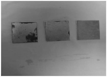
Embodiment 2

[0043] A ceramic-based circuit board, the preparation process of which is:

[0044] Use the OFC oxygen-free copper sheet with a size of 180mm×218mm and a thickness of 450μm, first clean it with pure water ultrasonically, then dry it, and then conduct vacuum plasma magnetron sputtering Cu plating on both sides of the copper sheet 2 O, to form a 3 μm dense Cu on its surface 2 O film;

[0045] The size is 184mm×222mm, the thickness is 1520μm, and the Al content is 80%. 2 o 3 The ceramic sheet is ultrasonically cleaned with pure water and then dried. The ceramic sheet and the copper sheet are stacked and placed in a transmission mesh belt atmosphere tunnel furnace, and the temperature is raised by a stepwise intermittent heating method, specifically: at 28°C / min Raise the temperature from room temperature to 440°C at a speed of 440°C, and keep it for 3-5 minutes; raise the temperature at a speed of 42°C / min to 810°C, and keep it for 5 minutes; raise the temperature at a speed o...


PUM

PropertyMeasurementUnit
thicknessaaaaaaaaaa
thicknessaaaaaaaaaa
thicknessaaaaaaaaaa

Abstract

The invention provides a preparation process of a ceramic-based circuit board and a product, and relates to the technical field of circuit boards. The invention relates to a preparation process of a ceramic-based circuit board, which comprises the following steps of: performing vacuum plasma magnetron sputtering of Cu2O on the surface of a copper sheet to form a layer of Cu2O film; placing the ceramic substrate on a copper sheet, and carrying out bonding by adopting a stepped intermittent heating method to obtain a circuit substrate; then cooling the circuit substrate by adopting a stepped intermittent cooling method; and recrystallizing the copper surface of the circuit substrate by adopting a high-low temperature alternating method, and cooling to obtain the ceramic-based circuit board. According to the method, continuous dynamic bonding is carried out by adopting a stepped intermittent heating method and a stepped intermittent cooling method, so that the stress generated when the copper sheet is combined with the ceramic can be released to the maximum extent, and the bending phenomenon caused by the stress generated due to different expansion coefficients of the two materials is eliminated.

Description

technical field [0001] The invention relates to the technical field of circuit boards, in particular to a preparation process and product of a ceramic-based circuit board. Background technique [0002] The circuit board is suitable for use with electronic components. The traditional structure of the circuit board is relatively simple, which makes the heat dissipation performance of the circuit board poor. When the circuit board is used for a long time, the internal components are damaged due to the high temperature, and the circuit board needs to be replaced continuously, increasing Therefore, it is necessary to improve the circuit board to make the heat dissipation effect of the circuit board better. [0003] Ceramic-based circuit boards are widely used in various electronic products due to their excellent thermal conductivity, extremely small thermal expansion coefficient, low dielectric constant and connection loss. The preparation methods of traditional ceramic substrat...

Claims


Application Information

Patent Timeline
Patent Type & Authority Applications(China)
IPC IPC(8): H05K3/00H05K3/02
CPCH05K3/0061H05K3/022
Inventor 高奉昌李长花张燕燕
Owner 青州云领电子科技有限公司
Why Eureka
Try Eureka