Method of manufacturing semiconductor device

Active Publication Date: 2017-06-15
DENSO CORP
View PDF3 Cites 0 Cited by
  • Summary
  • Abstract
  • Description
  • Claims
  • Application Information

AI Technical Summary

Benefits of technology

[0011]According to the above-described manufacturing method, the surface roughness of one principal surface of the semiconductor substrate is uniformized prior to the e

Problems solved by technology

In a case of the reverse conducting IGBT described above, since shadows appear on the front surface of the rear electrode corresponding to the patterns of the collector region and the cathode region, it is difficult to distinguish between such shadows and

Method used


Image

  • Method of manufacturing semiconductor device
  • Method of manufacturing semiconductor device
  • Method of manufacturing semiconductor device

Examples


Example

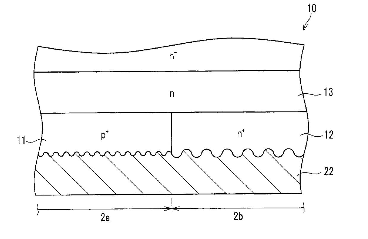
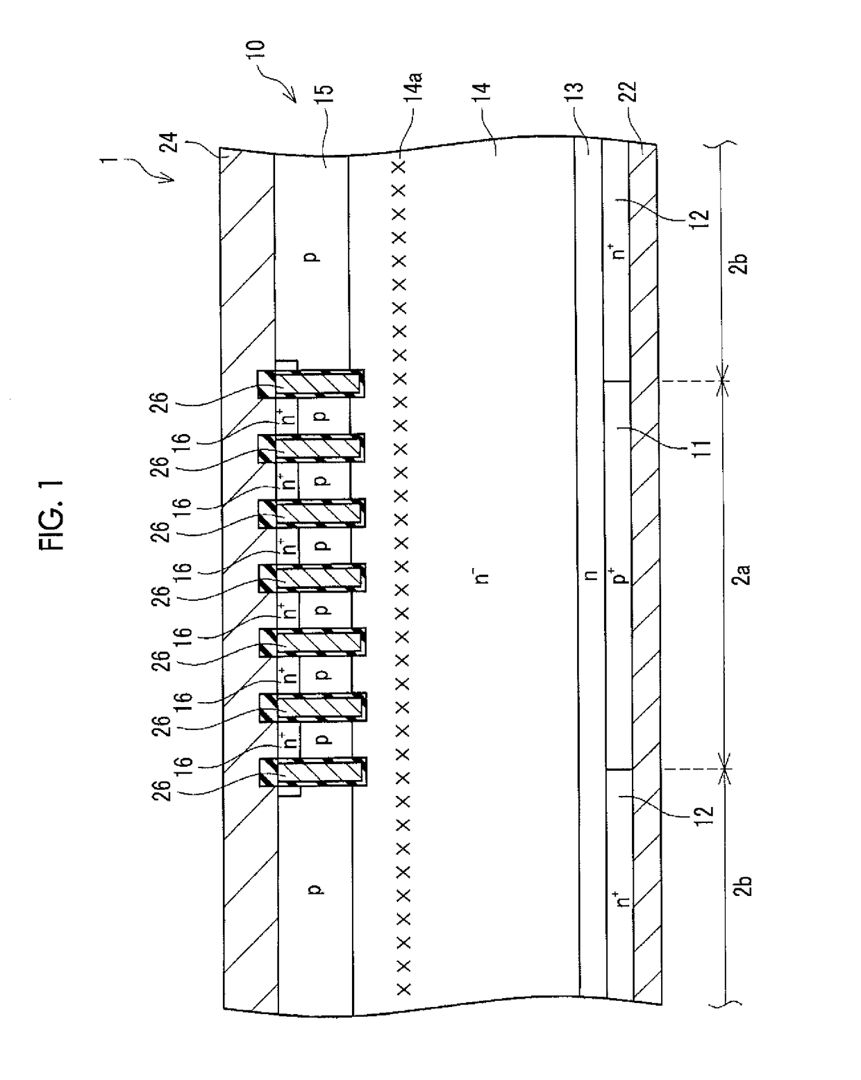
[0020]As shown in FIG. 1, a reverse conducting IGBT 1 includes a silicon single crystal semiconductor substrate 10 which is divided into an IGBT region 2a and a diode region 2b, a rear electrode 22 which covers the rear surface of the semiconductor substrate 10, a front electrode 24 which covers the front surface of the semiconductor substrate 10, and trench gates 26 which are provided on the front surface side of the IGBT region 2a of the semiconductor substrate 10. The rear electrode 22 functions as a collector electrode in the IGBT region 2a, and functions as a cathode electrode in the diode region 2b. The front electrode 24 functions as an emitter electrode in the IGBT region 2a, and functions as an anode electrode in the diode region 2b. In an example, aluminum silicon (AlSi) is used as the material of the rear electrode 22, and aluminum silicon (AlSi) is used as the material of the front electrode 24.

[0021]The semiconductor substrate 10 has a p+-type collector region 11, an n+...


PUM


Abstract

A method of manufacturing a semiconductor device includes a semiconductor region forming process, a cleaning process, a surface roughness uniformizing process, and an electrode forming process. As the semiconductor region forming process, semiconductor regions are formed such that a plurality of semiconductor regions with different ion injection amounts are exposed on one principal surface of a semiconductor substrate. As the cleaning process, after the semiconductor region forming process, a cleaning using hydrofluoric acid is performed on the one principal surface of the semiconductor substrate. As the surface roughness uniformizing process, after the cleaning process, the surface roughness of the one principal surface of the semiconductor substrate is uniformized. As the electrode forming process, after the surface roughness uniformizing process, electrodes are formed on the one principal surface of the semiconductor substrate.

Description

[0001]The disclosure of Japanese Patent Application No. 2015-242605 filed on Dec. 11, 2015 including the specification, drawings and abstract is incorporated herein by reference in its entirety.BACKGROUND[0002]1. Technical Field[0003]A technique disclosed in this specification relates to a method of manufacturing a semiconductor device.[0004]2. Description of Related Art[0005]In many semiconductor devices, electrodes are formed on one principal surface of a semiconductor substrate. Such electrodes are formed on one principal surface of the semiconductor substrate after one principal surface of the semiconductor substrate is cleaned. Japanese Patent Application Publication No. 2008-085050 (JP 2008-085050 A) discloses a technique which removes a natural oxide film formed on one principal surface of a semiconductor substrate using HF cleaning (cleaning using hydrofluoric acid) and then forms electrodes on one principal surface of the semiconductor substrate.SUMMARY[0006]As an example o...

Claims


Application Information

Patent Timeline
IPC IPC(8): H01L21/02H01L29/66H01L29/34H01L21/285
CPCH01L21/02068H01L29/34H01L29/66325H01L21/28556H01L21/02041H01L21/02057H01L21/28H01L21/0209H01L29/417H01L29/66348H01L29/7397H01L29/0834H01L29/1095H01L21/02049H01L21/02052H01L21/28044H01L21/2855H01L21/324H01L21/76859H01L29/7393
Inventor KAMEYAMA, SATORUAJIOKA, MASAKIOKI, SHUHEI
Owner DENSO CORP
Why Eureka
Try Eureka