Tandem organic photovoltaic devices that include a metallic nanostructure recombination layer
- Summary
- Abstract
- Description
- Claims
- Application Information
AI Technical Summary
Benefits of technology
Problems solved by technology
Method used
Image
Examples
Embodiment Construction
[0023]Organic photovoltaic devices and methods for forming the same are described herein in various embodiments. It should be understood that variations are possible within each of these embodiments and in other embodiments not specifically described for the sake of clarity and / or to avoid redundancy within this disclosure. Additionally, the order, extent, and composition of the various layers and structures disclosed herein can be varied, altered, divided, or subdivided to meet varying performance specifications.
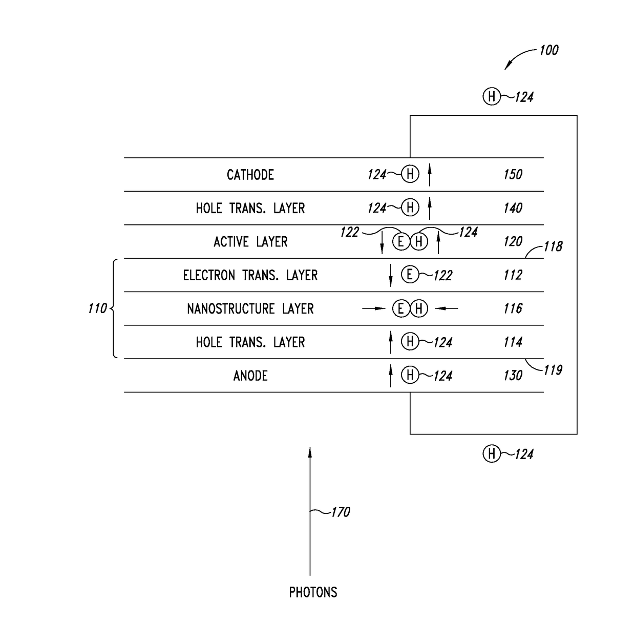
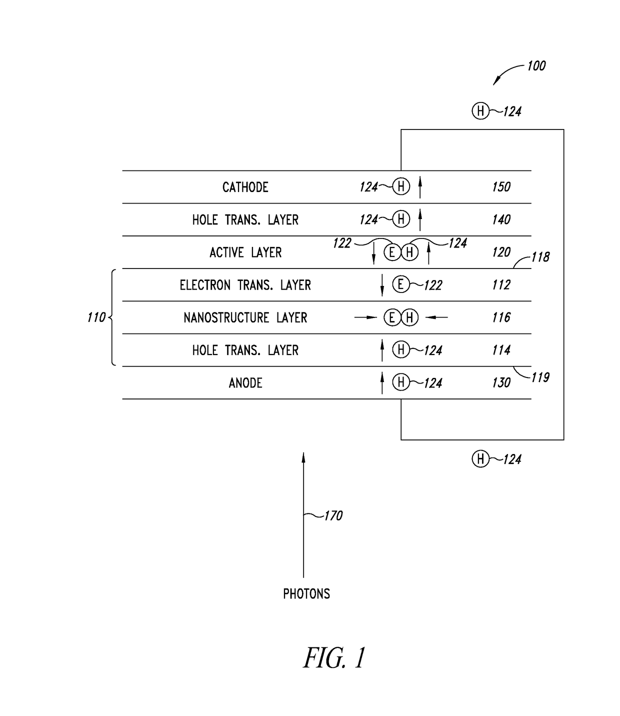
[0024]FIG. 1 illustrates an organic photovoltaic device comprising an intermediate layer 110 that includes an electron transport layer 112, a hole transport layer 114, and a metallic nanostructure layer 116 interposed between the active layer 120 and a first electrode 130 of a single junction organic photovoltaic 100. The single junction organic photovoltaic 100 further includes a hole transport layer 140 deposited between the active layer 120 and a second electrode 150.
[00...
PUM
| Property | Measurement | Unit |
|---|---|---|
| Fraction | aaaaa | aaaaa |
| Fraction | aaaaa | aaaaa |
| Fraction | aaaaa | aaaaa |
Abstract
Description
Claims
Application Information


