Organic light emitting display panel and manufacturing method thereof, and display device

a technology of light-emitting display panel and organic light-emitting layer, which is applied in the field of display technology, can solve the problems of low light-emitting layer utilization rate and large power consumption of organic light-emitting layer, and achieve the effect of increasing the light-emitting rate of organic light-emitting uni

Active Publication Date: 2017-06-22
BOE TECH GRP CO LTD
View PDF2 Cites 38 Cited by
  • Summary
  • Abstract
  • Description
  • Claims
  • Application Information

AI Technical Summary

Benefits of technology

[0040]In the organic light emitting display panel and the manufacturing method thereof, and the display device of the invention, since the quantum material layer exhibiting quantum size effects is arranged on a side of the color filter substrate close to the array substrate or on a side of the array substrate close to the color filter substrate, and the photolu

Problems solved by technology

However, due to the fact that only a part of light emitted from the organic light emitting layer passes through the color

Method used


Image

  • Organic light emitting display panel and manufacturing method thereof, and display device
  • Organic light emitting display panel and manufacturing method thereof, and display device
  • Organic light emitting display panel and manufacturing method thereof, and display device

Examples


first embodiment

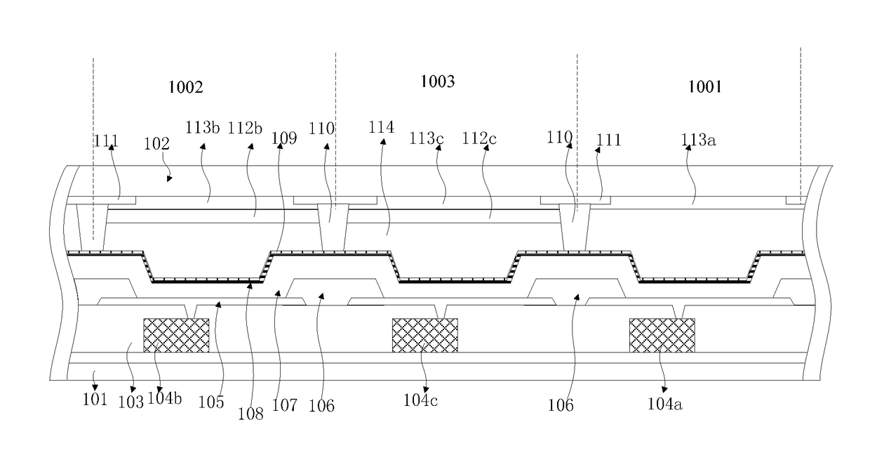
[0050]As shown in FIG. 1, the embodiment provides an organic light emitting display panel, including: an array substrate and a color filter substrate arranged opposite to each other; an organic light emitting unit, which is arranged on a side of the array substrate close to the color filter substrate, the array substrate being configured to control the organic light emitting unit to emit light; and a plurality of pixel units arranged in a matrix formed by the array substrate and the color filter substrate, and each pixel unit including a plurality of sub-pixels;

[0051]wherein, the organic light emitting display panel further includes a quantum material layer at a sub-pixel region where a color of light emitted from the organic light emitting unit is not consistent with a color of the sub-pixel and a wavelength of light emitted from the organic light emitting unit is smaller than a wavelength of the color of the sub-pixel, and the quantum material layer is provided on a side of the co...

second embodiment

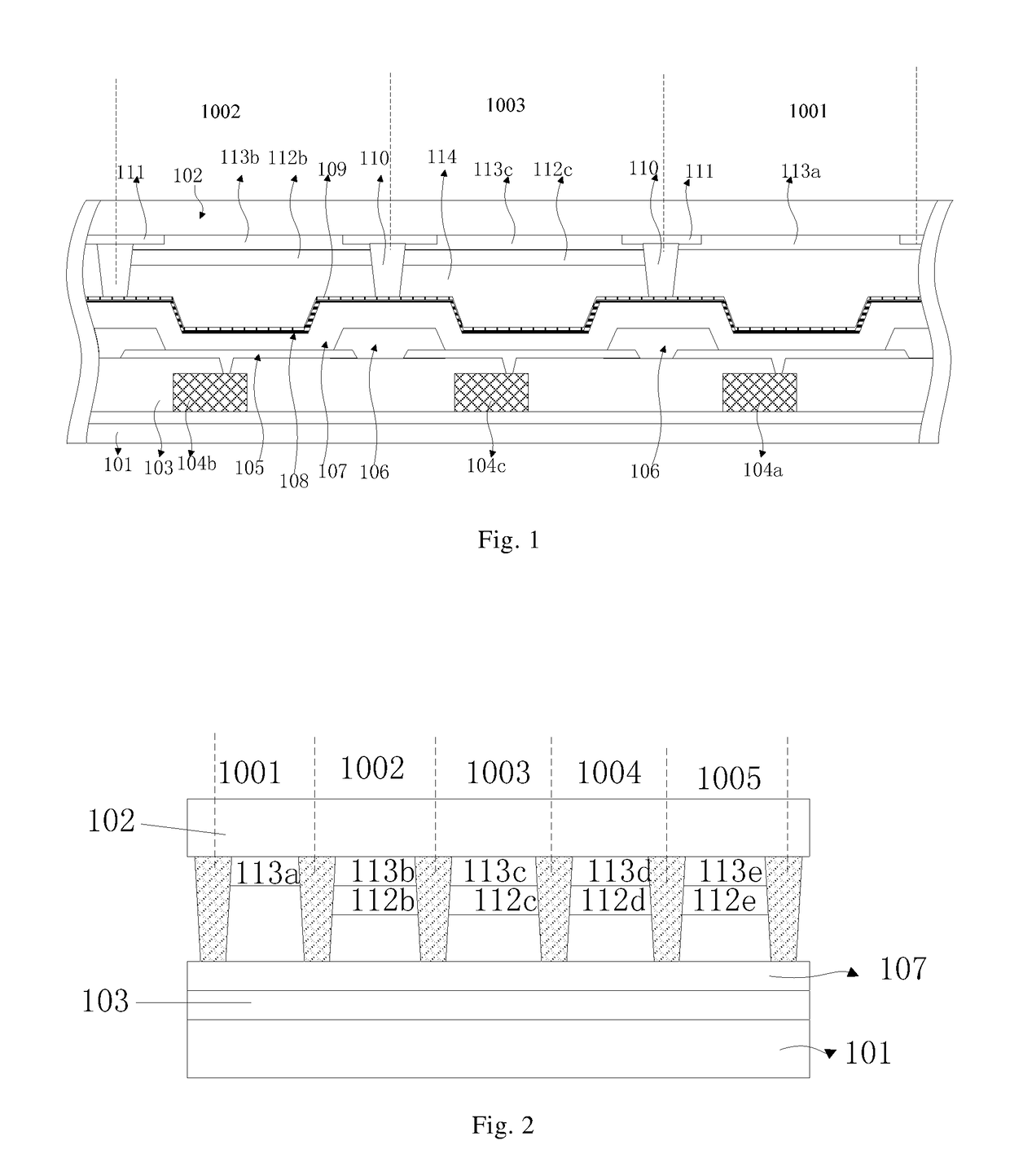
[0079]As shown in FIG. 2, in a first method for preparing the top-emission type organic light emitting display panel, the quantum material layer is first prepared on the color filter substrate, and the array substrate and the color filter substrate are assembled.

[0080]In particular, the above method for preparing the top-emission type organic light emitting display panel includes the following steps:

[0081]S1: preparing an array substrate;

[0082]An array backplate 103 (including a thin film transistor 104 and an anode) is prepared on a glass substrate 101 to form the array substrate, and it should be understood that, the method for preparing the array substrate belongs to the prior art, and will not be elaborated herein.

[0083]S2: preparing an organic light emitting layer on the array substrate;

[0084]In this embodiment, a vacuum evaporation method is used to form the organic light emitting layer 107, in particular, the organic light emitting layer 107 of several colors are simultaneous...

third embodiment

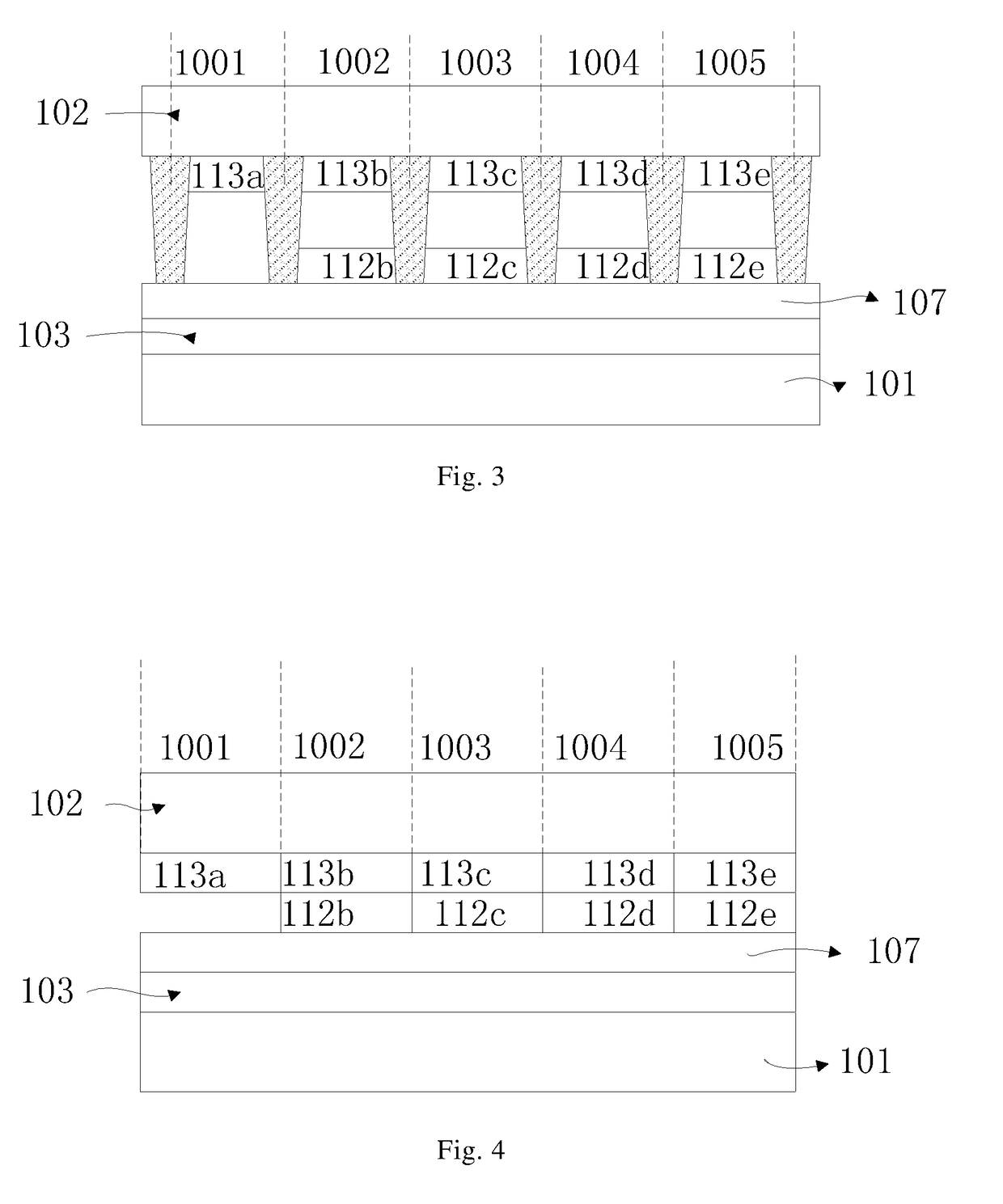
[0102]As shown in FIG. 3, in a second method for preparing the top-emission type organic light emitting display panel, the organic light emitting layer and the quantum material layer are sequentially prepared on the array substrate, and the array substrate and the color filter substrate are assembled.

[0103]In particular, the above method for preparing the top-emission type organic light emitting display panel includes the following steps:

[0104]S1: preparing an array substrate;

[0105]An array backplate 103 (including a thin film transistor 104 and an anode) is prepared on a glass substrate 101 to form the array substrate, and it should be understood that, the method for preparing the array substrate belongs to the prior art, and will not be elaborated herein.

[0106]S2: preparing an organic light emitting layer on the array substrate;

[0107]In this embodiment, a vacuum evaporation method is used to form the organic light emitting layer 107, in particular, the organic light emitting layer...


PUM


Abstract

The invention provides an organic light emitting display panel and a manufacturing method thereof, and a display device. In the organic light emitting display panel and the manufacturing method thereof, and the display device of the invention, since a quantum material layer exhibiting quantum size effects is arranged on a side of a color filter substrate close to an array substrate or on a side of an array substrate close to a color filter substrate, and can convert a part of light emitted thereinto from the organic light emitting unit into light with a same color as that of a corresponding sub-pixel, the utilization rate of light emitted from the organic light emitting unit is increased, brightness is improved, and power consumption is reduced.

Description

FIELD OF THE INVENTION[0001]The invention relates to the field of display technology, and particularly to an organic light emitting display panel and a manufacturing method thereof, and a display device.BACKGROUND OF THE INVENTION[0002]A quantum dot material refers to a material exhibiting quantum size effects in three dimensions, that is, the characteristic size of the material is comparable to the electron De Broglie wavelength, the coherent wavelength and the exciton Bohr radius, the electrons are confined in nanospace, the electron transport is restricted, the average free path of the electron is very short, locality and coherence of the electrons are enhanced, and at this time, a quasi continuous band is evolved into a discrete energy level structure. This special energy level structure makes the quantum dots have photoluminescence and electroluminescence properties. The luminescence spectra can be prepared by controlling structure, material and particle size of the quantum dot...

Claims


Application Information

Patent Timeline
IPC IPC(8): H01L51/52H01L51/56H01L51/00H01L27/32
CPCH01L51/5281H01L27/322H01L51/0019H01L51/56H01L27/3213H10K59/351H10K59/38H10K50/86H10K2102/331H10K71/00H10K71/236
Inventor XU, XIANBIN
Owner BOE TECH GRP CO LTD
Why Eureka
Try Eureka