Scanning electron microscope and method for controlling same

a scanning electron microscope and electron microscope technology, applied in the direction of instruments, material analysis, material analysis using wave/particle radiation, etc., can solve the problems of increased demand for quantitative analysis, difficult to interpret image contrast,

Active Publication Date: 2017-06-29
HITACHI HIGH-TECH CORP
View PDF4 Cites 7 Cited by
  • Summary
  • Abstract
  • Description
  • Claims
  • Application Information

AI Technical Summary

Benefits of technology

[0014]According to the present invention, it is possible to perform the energy dispersion of the secondary electron, without changing the number of electrons injected into the electrometer and the energy resolution even if the retarding voltage Vr is changed, by using the retarding method.

Problems solved by technology

On the other hand, it is difficult to interpret the image contrast and there is an increased demand for a quantitative analysis of the energy of secondary electrons detected by the SEM.

Method used


Image

  • Scanning electron microscope and method for controlling same
  • Scanning electron microscope and method for controlling same
  • Scanning electron microscope and method for controlling same

Examples


first embodiment

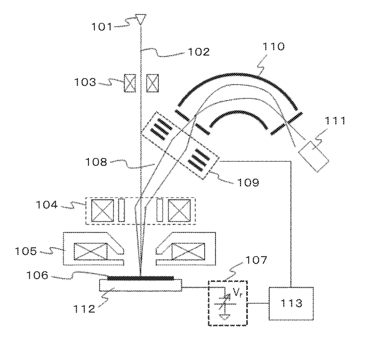
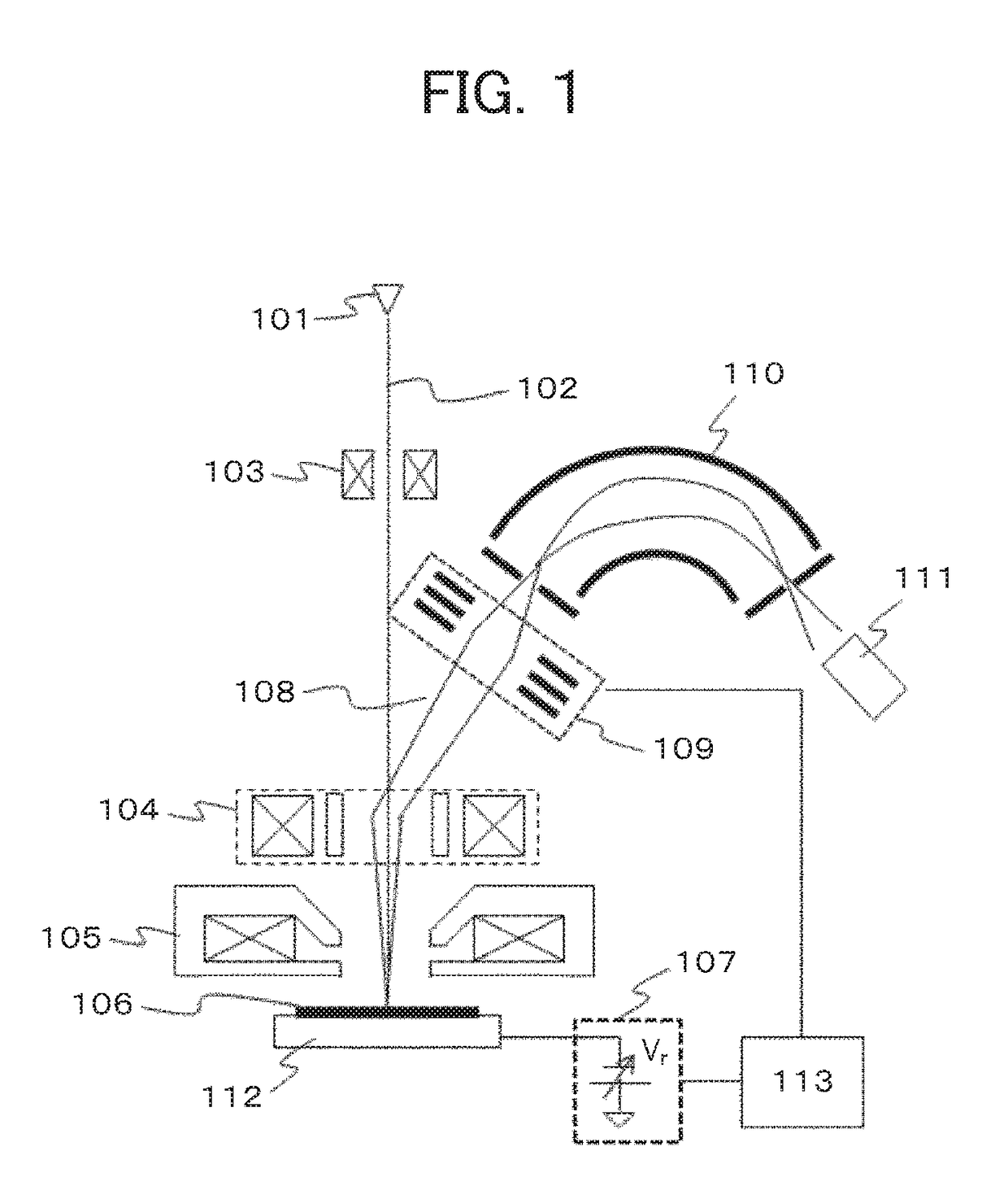
[0026]The first describes an example of an SEM, as a first embodiment, including: an electron source; a first deflector that deflects a first electron beam emitted from the electron source; a converging lens that focuses the primary electron beam deflected by the first deflector; a second deflector that deflects a secondary electron from a sample, which is generated by the focused primary electron beam; a voltage applying unit that applies a negative voltage to the sample to decelerate the primary electron beam; a spectrometer for dispersing the secondary electron; a detector that detects the secondary electron passing through the spectrometer; an electrostatic lens provided between the second deflector and the spectrometer; and a voltage control unit that controls the voltage applied to the electrostatic lens based on the negative voltage applied to the sample. The electrostatic lens allows the deflecting action to be overlapped with the converging action.

[0027]FIG. 1 is a diagram ...

second embodiment

[0044]The second embodiment is an example of an SEM in which a negative second bias voltage is applied to the entire spectrometer which is then floated, and in which the bias voltage is controlled according to the negative retarding voltage applied to the sample. In the SEM, the voltage for discriminating the secondary electron by energy is superimposed with the negative second bias voltage. Further, the SEM also includes an input unit for the user to input the energy resolution of the spectrometer, so that the difference between the negative second bias voltage applied to the spectrometer and the negative voltage applied to the sample is controlled according to the value of the energy resolution that is input from the input unit.

[0045]FIG. 5 shows the configuration of the SEM according to the second embodiment. As shown in the figure, the SEM according to the present embodiment is configured by adding a bias power supply B501, a ΔE input unit 502, a spectrometer power supply A503, ...

third embodiment

[0057]The third embodiment is an example of an SEM which also includes a potential meter that measures the surface potential of the sample, measuring the potential of the sample by the potential meter before irradiation of the primary electron on the sample, to change the negative bias voltage in conjunction with changes in the potential of the sample. FIG. 7 is a diagram of the configuration of the SEM according to the present embodiment, in which a potential meter 701 is added to the configuration of the second embodiment shown in FIG. 5.

[0058]When an insulator is observed by the SEM, the retarding voltage Vr that is applied to the sample holder 112 by the retarding power supply 107 may differ from the potential Vs of the sample surface. If the voltage Vr is different from the potential Vs, the bias voltages Vb1 and Vb2 may deviate from the optimal points because the bias voltages Vb1 and Vb2 are controlled with respect to the retarding voltage Vr in the configurations of the firs...


PUM

PropertyMeasurementUnit
incident energyaaaaaaaaaa
thicknessaaaaaaaaaa
scanning electron microscopeaaaaaaaaaa

Abstract

The scanning electron microscope includes: an electron source; a first deflector for deflecting a primary electron beam emitted from the electron source; a second deflector for focusing the primary electron beam deflected by the first deflector and deflecting a second electron from a sample, which is generated the focused primary electron beam, to the outside of the optical axis; a voltage applying unit for applying a negative voltage to the sample to decelerate the primary electron beam; a spectrometer for dispersing the secondary electron; a detector for detecting the secondary electron passing through the spectrometer; an electrostatic lens provided between the second deflector and the spectrometer; and a voltage control unit that controls the voltage applied to the electrostatic lens based on the negative voltage applied to the sample. The electrostatic lens allows the deflecting action to be overlapped with the converging action.

Description

TECHNICAL FIELD[0001]The present invention relates to a scanning electron microscope that produces an image by the signal of electrons such as secondary electrons from a sample by irradiating the sample with an electron beam while scanning the electron beam. More particularly, the present invention relates to a spectroscopic technique for detecting secondary electrons by discriminating them by energy.BACKGROUND ART[0002]Currently, the scanning electron microscope (hereinafter, SEM) is widely used in observation of submicron- and nano-sized samples. The SEM is designed to form an image by irradiating a sample with primary electrons emitted from an electron source while scanning the primary electrons, and by detecting secondary electrons that are generated in the sample. Here, the secondary electrons can be grouped into “true” secondary electrons characterized by having an energy of 50 eV or less, and backscattered electrons having an energy nearly equal to the incident energy of the ...

Claims


Application Information

Patent Timeline
Patent Type & Authority Applications(United States)
IPC IPC(8): H01J37/28G01N23/225H01J37/26
CPCH01J37/28H01J37/263G01N23/2251H01J2237/2806H01J2237/28H01J2237/2801H01J2237/2602H01J49/48H01J37/244H01J37/1472H01J37/12H01J2237/24485H01J2237/1202H01J2237/1504
Inventor SHIRAHATA, KAORIBIZEN, DAISUKESAKAKIBARA, MAKOTOSOHDA, YASUNARIKAWANO, HAJIMEKAZUMI, HIDEYUKI
Owner HITACHI HIGH-TECH CORP
Why Eureka
Try Eureka