
Semiconductor device

a technology of semiconductor devices and semiconductors, applied in semiconductor devices, semiconductor/solid-state device details, electrical apparatus, etc., can solve the problems of increasing the stiffness of the terminal, increasing the stress applied, and becoming more and more difficult to fabricate elements that meet the conditions, so as to reduce the area of each bonding portion, reduce the absolute value of thermal stress applied to each bonding portion, and suppress the peeling effect of the bonding fa

Inactive Publication Date: 2017-07-20
MITSUBISHI ELECTRIC CORP
View PDF5 Cites 2 Cited by
  • Summary
  • Abstract
  • Description
  • Claims
  • Application Information

AI Technical Summary

Benefits of technology

The present invention is a semiconductor device that has multiple ultrasonically bonding portions on its surface. By using this design, the area of each bonding portion is reduced, which reduces the thermal stress applied to each bonding portion and suppresses peeling of the bonding face. Additionally, the overall area of the bonding portions increases, resulting in a more reliable semiconductor device. The invention also facilitates positioning of the electrode terminal with respect to the conductive pattern by fit between the projection and depression on the surface, ensuring stable ultrasonic bonding and high bonding reliability.

Problems solved by technology

Since conventional solder-bonding techniques cannot ensure reliability of soldering materials under high temperatures, it is becoming more and more difficult to fabricate the elements that satisfy the conditions.
The increase in size of the electrode terminal causes an increase of the stiffness of the terminal.
This results in an increase of a stress applied to the bonding portion accompanied by displacement of a package due to the heat generated by operation of the power semiconductor element, and thus a problem, such as reduction of bonding strength and terminal peeling, may occur.
Further, due to an increase in the thickness of the electrode terminal and the area of a bonding face, it becomes harder to propagate the energy of the ultrasonic bonding to the bonding face.
However, the increase of these elements may cause a problem, i.e., the insulating substrate provided under the conductive pattern is damaged.

Method used


Image

  • Semiconductor device
  • Semiconductor device
  • Semiconductor device

Examples


first embodiment

[0048]

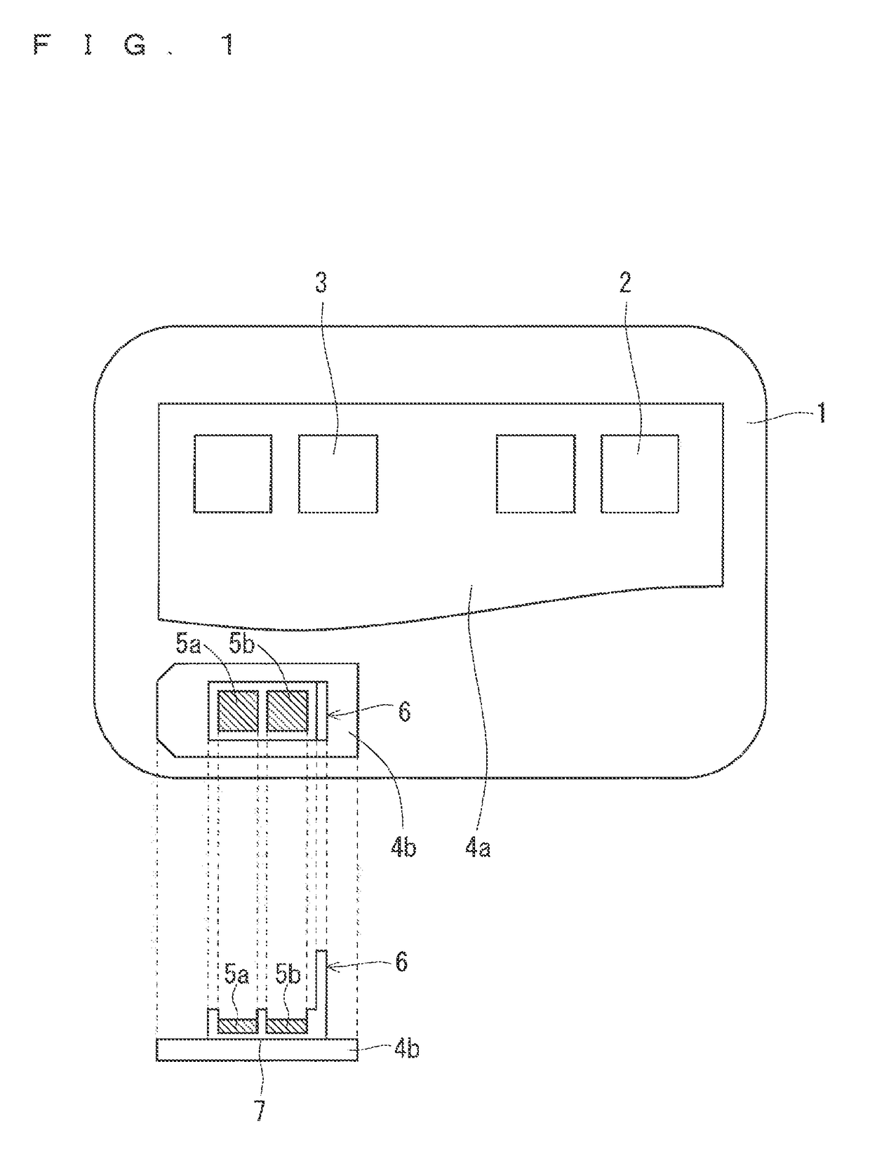
[0049]FIG. 1 is a plan view and a front view of a structure of a semiconductor device according to a first embodiment. FIG. 2 is a perspective view of an electrode terminal 6 and a conductive pattern 4b. In this first embodiment, like in the prerequisite art (FIG. 14), conductive patterns 4a and 4b are disposed on the insulating substrate 1, and semiconductor elements (a MOSFET chip 2 and an SBD chip 3) are bonded to the conductive pattern 4a. The electrode terminal 6 is bonded on the conductive pattern 4b.

[0050]According to the prerequisite art, ultrasonic bonding is performed at only one position on one bonding face between the electrode terminal 6 and the conductive pattern 4b. Accordingly, a recess 5 is formed by the ultrasonic bonding at one position on the upper surface of a bonding portion of the electrode terminal 6.

[0051]On the other hand, according to this first embodiment, as shown in FIG. 1, a plurality of bonding portions are provided on one bonding face 7 of the...

second embodiment

[0059]

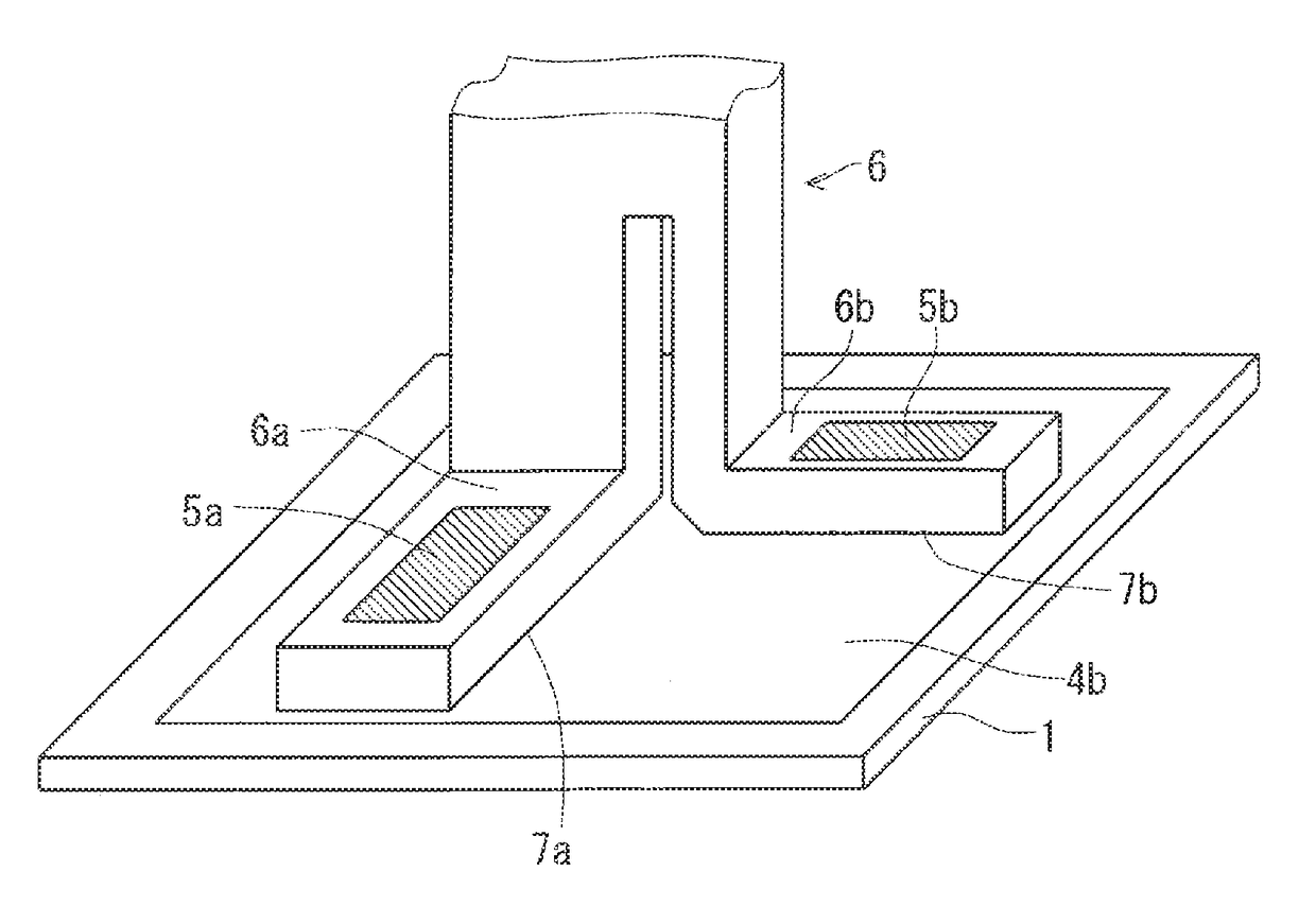
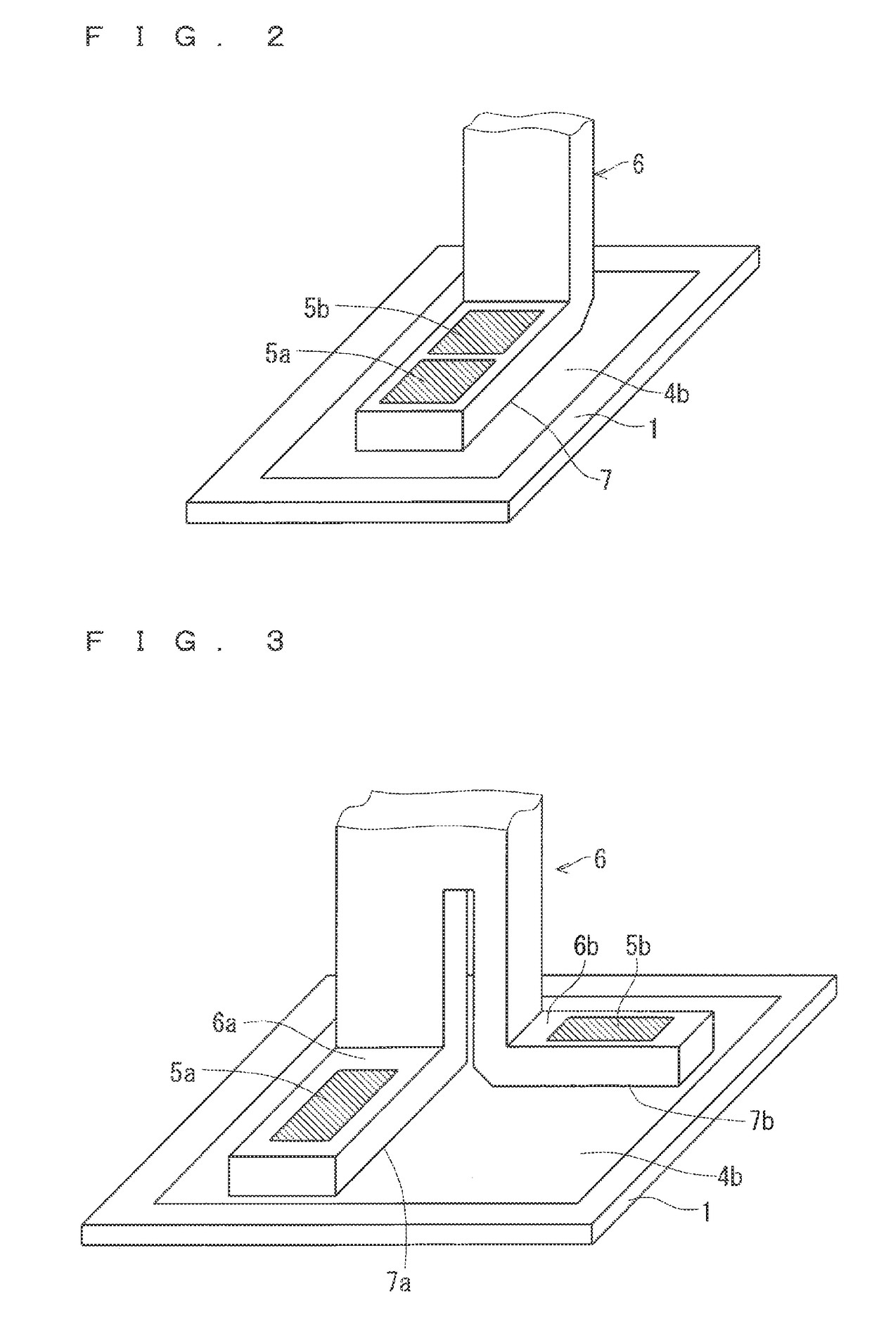
[0060]FIG. 3 is a perspective view of an electrode terminal 6 and a conductive pattern 4b according to a second embodiment. In this second embodiment, the electrode terminal 6 is a flat plate. The root of the electrode terminal 6 is divided into two branches in the width direction. In other words, the root of the electrode terminal 6 includes two branches 6a, 6b.

[0061]As shown in FIG. 3, the branches 6a, 6b are bent to form an angle of 90° with each other in a plan view. The branch 6a is bonded to the conductive pattern 4b by ultrasonic bonding on the bonding face 7a. In the same manner, the branch 6b is bonded by the ultrasonic bonding to the conductive pattern 4b on the bonding face 7b. On the bonding faces 7a, 7b, the branches 6a, 6b are respectively bonded by the ultrasonic bonding to the conductive pattern 4b at one position. Recesses 5a, 5b are formed by the ultrasonic bonding at the upper surfaces of the branches 6a, 6b.

[0062]

[0063]In this second embodiment, the secti...

third embodiment

[0075]

[0076]FIG. 4 is a perspective view of an electrode terminal 6 and a conductive pattern 4b according to a third embodiment. In this third embodiment, the electrode terminal 6 is a flat plate. The root of the electrode terminal 6 is divided into two branches in the thickness direction. In other words, the root of the electrode terminal 6 includes two branches 6a, 6b.

[0077]As shown in FIG. 4, the branches 6a, 6b are bent in opposite directions to form an angle of 180° with each other in a plan view. The branch 6a is bonded to the conductive pattern 4b by ultrasonic bonding on the bonding face 7a. Similarly, the branch 6b is bonded by the ultrasonic bonding to the conductive pattern 4b on the bonding face 7b. Each of the branches 6a, 6b is bonded by the ultrasonic bonding to the conductive pattern 4b at one position on one of the bonding faces 7a, 7b. The total sum of the areas of the bonding faces 7a, 7b according to this third embodiment is twice as large as that of the bonding...


PUM


Abstract

An object of the present invention is to obtain a semiconductor device having highly reliable bonding portions. The semiconductor device according to the present invention includes an insulating substrate on which a conductive pattern is formed, and an electrode terminal and a semiconductor element which are bonded to the conductive pattern, the electrode terminal and the conductive pattern are bonded by ultrasonic bonding on a bonding face, and the ultrasonic bonding is performed at a plurality of positions.

Description

TECHNICAL FIELD[0001]The present invention relates to a semiconductor device, particularly to a semiconductor device to which an electrode terminal is bonded by ultrasonic bonding.BACKGROUND ART[0002]Nowadays, power semiconductor devices are necessary equipment in many different fields from small-sized electronic devices to automobiles, bullet trains, etc., and also to electric power transmission and distribution. The use areas and application fields have been increasing year by year, and in the fields of automobiles, bullet trains, electric power, and the like, higher current, higher breakdown voltage, and operation temperatures in a wide range, especially durability under high operation temperatures have been desired, not to mention high reliability and long lifetime. Since conventional solder-bonding techniques cannot ensure reliability of soldering materials under high temperatures, it is becoming more and more difficult to fabricate the elements that satisfy the conditions. As ...

Claims


Application Information

Patent Timeline
Patent Type & Authority Applications(United States)
IPC IPC(8): H01L23/00H01L21/48H01L23/495
CPCH01L23/562H01L23/49517H01L21/4839H01L21/4825H01L23/49558H01L25/18H01L2924/181H01L2224/48091H01L2224/48137H01L2224/73265H01L2224/32225H01L23/24H01L23/49811H01L24/29H01L24/32H01L24/45H01L24/48H01L24/73H01L24/83H01L25/072H01L2224/291H01L2224/29139H01L2224/32245H01L2224/45014H01L2224/45015H01L2224/45124H01L2224/45147H01L2224/45424H01L2224/8384H01L2924/10253H01L2924/10272H01L2924/1033H01L2924/12032H01L2924/13055H01L2924/13091H01L23/3735H01L2924/00012H01L2924/00014H01L2924/014H01L2224/48247H01L2924/2076H01L2924/206
Inventor KITAJIMA, YUMIEYANAGIMOTO, TATUNORIARAI, KIYOSHI
Owner MITSUBISHI ELECTRIC CORP
Learn More