
Multi-Layer Ceramic Electronic Component, Method of Producing the Same, and Ceramic Body

Inactive Publication Date: 2017-07-27
TAIYO YUDEN KK
View PDF17 Cites 17 Cited by
  • Summary
  • Abstract
  • Description
  • Claims
  • Application Information

AI Technical Summary

Benefits of technology

The patent text discusses the problem of micro irregularities and gaps that are generated on the side surfaces of multi-layer chips after cutting. These irregularities can lead to peeling off of the side margins and reduced joint strength. The technical effect of the patent is to provide a solution to prevent peeling off of the side margins in a subsequent step.

Problems solved by technology

In this case, micro irregularities are generated on side surfaces of multi-layer chips after cutting.
This leads to reduction in joint strength of the side margins to the multi-layer chip, and the side margins are easily peeled off from the multi-layer chip.

Method used


Image

  • Multi-Layer Ceramic Electronic Component, Method of Producing the Same, and Ceramic Body
  • Multi-Layer Ceramic Electronic Component, Method of Producing the Same, and Ceramic Body
  • Multi-Layer Ceramic Electronic Component, Method of Producing the Same, and Ceramic Body

Examples


Embodiment Construction

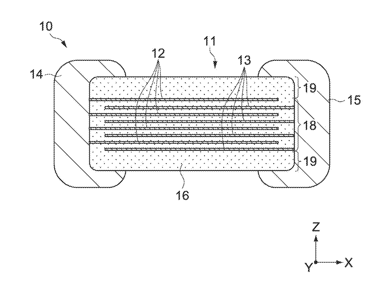
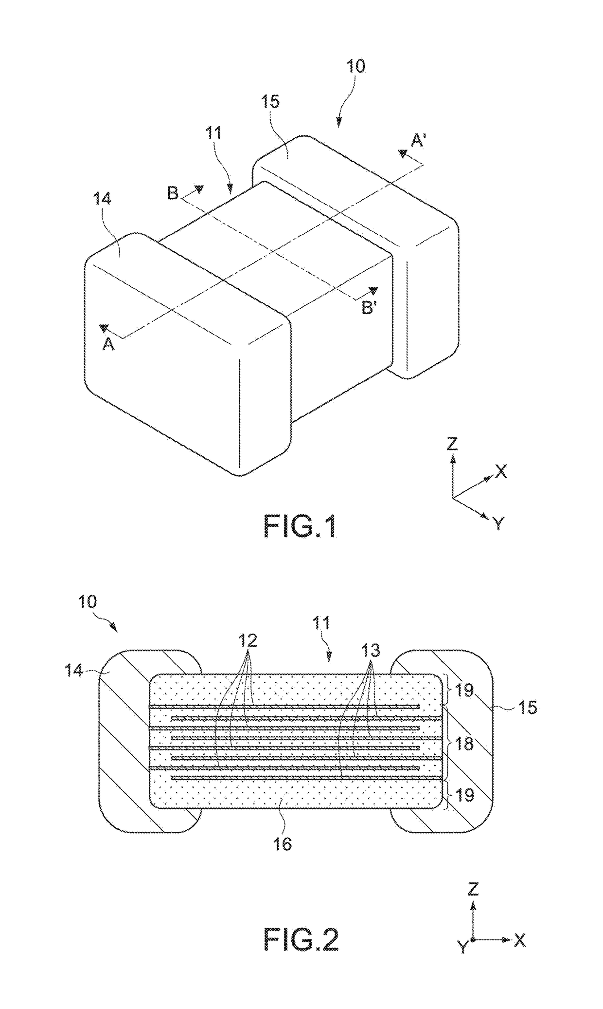
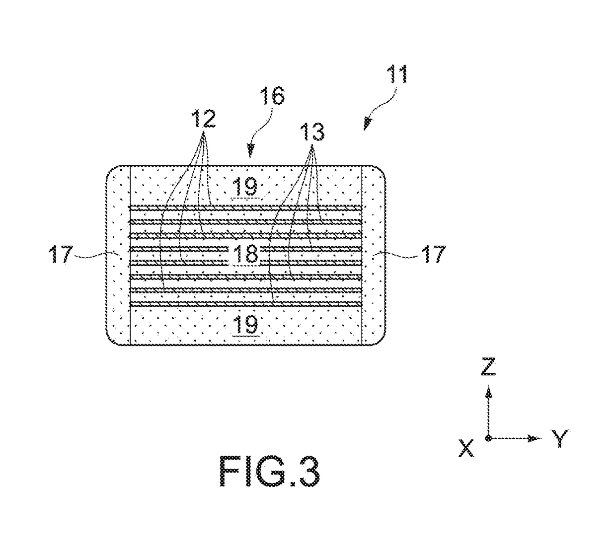
[0052]Hereinafter, embodiments of the present invention will be described with reference to the drawings.

[0053]In the figures, an X axis, a Y axis, and a Z axis orthogonal to one another are shown as appropriate. The X axis, the Y axis, and the Z axis are common in all figures.

1. Configuration of Multi-Layer Ceramic Capacitor 10

[0054]FIGS. 1 to 3 each show a multi-layer ceramic capacitor 10 according to an embodiment of the present invention. FIG. 1 is a perspective view of the multi-layer ceramic capacitor 10. FIG. 2 is a cross-sectional view of the multi-layer ceramic capacitor 10 taken along the A-A′ line in FIG. 1. FIG. 3 is a cross-sectional view of the multi-layer ceramic capacitor 10 taken along the B-B′ line in FIG. 1.

[0055]The multi-layer ceramic capacitor 10 includes a body 11, a first external electrode 14, and a second external electrode 15. The first external electrode 14 and the second external electrode 15 are apart from each other and face each other in an X-axis dir...


PUM

PropertyMeasurementUnit
Fractionaaaaaaaaaa
Fractionaaaaaaaaaa
Thicknessaaaaaaaaaa

Abstract

A method of producing a multi-layer ceramic electronic component includes: preparing a multi-layer sheet including laminated ceramic sheets, and internal electrodes disposed between the ceramic sheets; cutting the multi-layer sheet to produce multi-layer chips each having side surfaces from which the internal electrodes are exposed; smoothing the side surfaces of the multi-layer chips; and providing side margins to the smoothed side surfaces of the multi-layer chips.

Description

CROSS REFERENCE TO RELATED APPLICATION[0001]This application claims priority under 35 U.S.C. §119 to Japanese Patent Application No. 2016-012051, filed Jan. 26, 2016, which is hereby incorporated by reference in its entirety.BACKGROUND[0002]The present invention relates to a multi-layer ceramic electronic component including side margins provided in a subsequent step, to a method of producing the multi-layer ceramic electronic component, and to a ceramic body.[0003]Along with miniaturization and achievement of high performance of electronic devices, there have recently been increasingly strong demands for miniaturization and increase in capacity with respect to multi-layer ceramic capacitors used in the electronic devices. In order to meet those demands, it is effective to enlarge internal electrodes of the multi-layer ceramic capacitor. In order to enlarge the internal electrodes, it is necessary to thin side margins for ensuring insulation properties of the periphery of the intern...

Claims


Application Information

Patent Timeline
IPC IPC(8): H01G4/30H01G4/248H01G13/00H01G4/12H01G4/012
CPCH01G4/30H01G4/12H01G4/248H01G13/006H01G4/012H01G4/232Y10T29/43Y10T29/435
Inventor KATO, YOICHIMIZUNO, KOTAROKONISHI, YUKIHIRO
Owner TAIYO YUDEN KK
Features
  • Generate Ideas
  • Intellectual Property
  • Life Sciences
  • Materials
  • Tech Scout
  • Unparalleled Data Quality
  • Higher Quality Content
  • 60% Fewer Hallucinations
Learn More