

Scan driving circuit and NAND logic operation circuit thereof
a driving circuit and logic operation technology, applied in logic circuits, pulse techniques, instruments, etc., can solve the problems how to use a single type of device to manufacture inverters, etc., and the problem of urgently solving the problem of nand or nor
- Summary
- Abstract
- Description
- Claims
- Application Information
AI Technical Summary
Benefits of technology
Problems solved by technology
Method used
Image

Examples
Embodiment Construction
[0029]In the following, with reference to accompanying drawings of embodiments of the invention, technical solutions in the embodiments of the invention will be clearly and completely described. Apparently, the embodiments of the invention described below only are a part of embodiments of the invention, but not all embodiments. Based on the described embodiments of the invention, all other embodiments obtained by ordinary skill in the art without creative effort belong to the scope of protection of the invention.
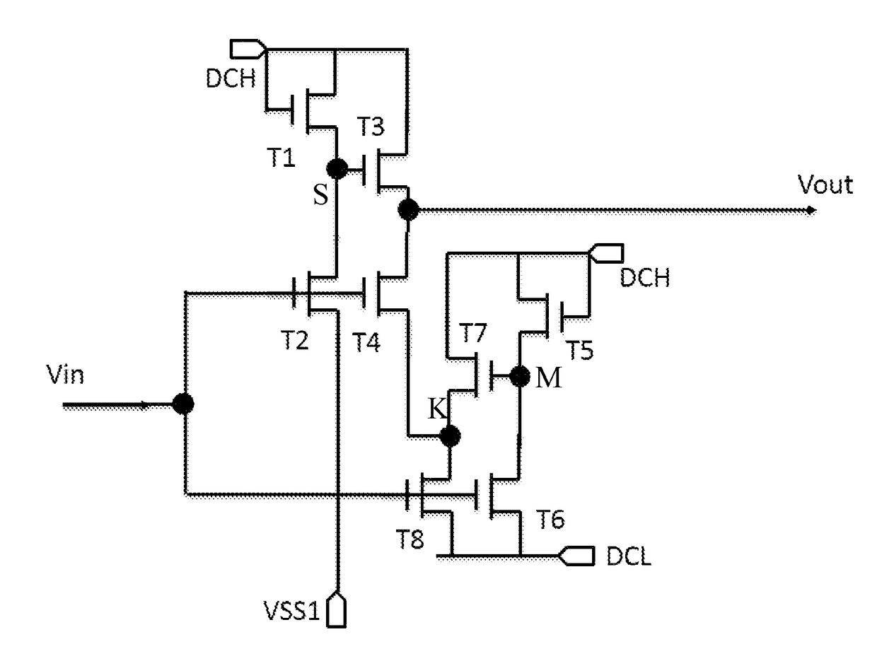
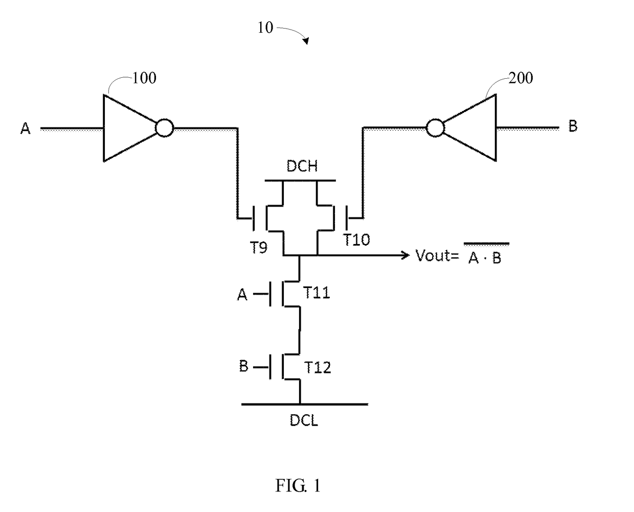
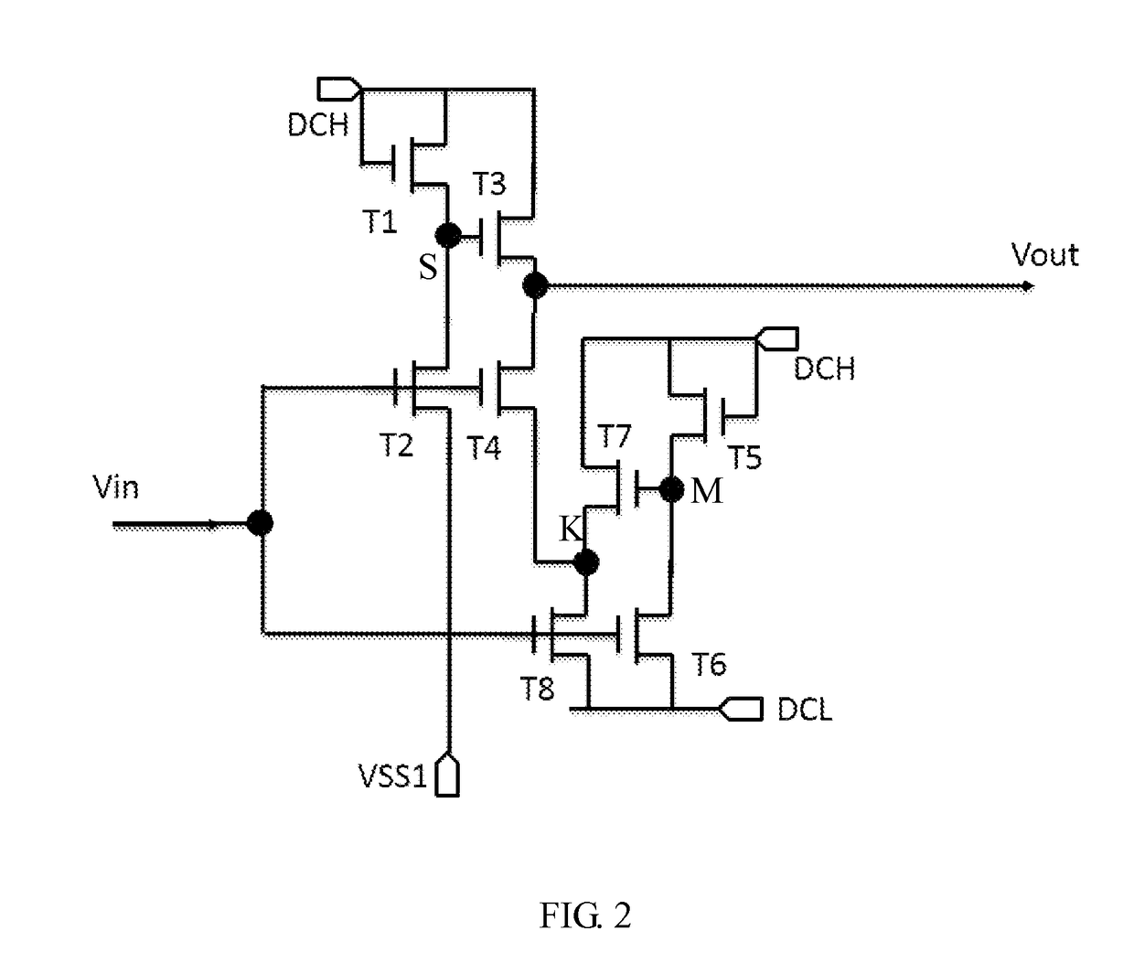
[0030]Referring to FIG. 1, a circuit diagram of a NAND logic operation circuit of an embodiment of the invention is shown. The NAND logic operation circuit 10 is a logic operation circuit applied to a scan driving circuit for an oxide semiconductor thin film transistor.
[0031]In particular, the circuit 10 includes a first inverter 100 and a second inverter 200. The first inverter 100 and the second inverter 200 both are inverters applied to a pull-down holding circuit of a GO...
PUM
| Property | Measurement | Unit |
|---|---|---|
| structures | aaaaa | aaaaa |
Abstract
Description
Claims
Application Information