Low Loss Multi-State Phase Shifter

a phase shifter and multi-state technology, applied in the field of programmable multi-state rf phase shifter circuits, can solve the problems of series-cell phase shifter architectures suffering from excessive insertion loss (il), il problem is exacerbated, return loss also becomes worse, etc., to reduce the number of series-connected, low insertion loss (il), and good return loss

Active Publication Date: 2017-08-10
PSEMI CORP
View PDF2 Cites 23 Cited by
  • Summary
  • Abstract
  • Description
  • Claims
  • Application Information

AI Technical Summary

Benefits of technology

[0011]The present invention encompasses a multi-state phase shifter circuit having both low insertion loss (IL) and good return loss. In preferred embodiments, two or more phase shift elements are combined into a single cell architecture to reduce ...

Problems solved by technology

Series-cell phase shifter architectures suffer from excessive insertion loss (IL) due to the cumulative IL of each switch Sna of the serially-connected phase shifter cells.
The IL problem is exacerbated when additional phase shifter...

Method used


Image

  • Low Loss Multi-State Phase Shifter
  • Low Loss Multi-State Phase Shifter
  • Low Loss Multi-State Phase Shifter

Examples


first embodiment

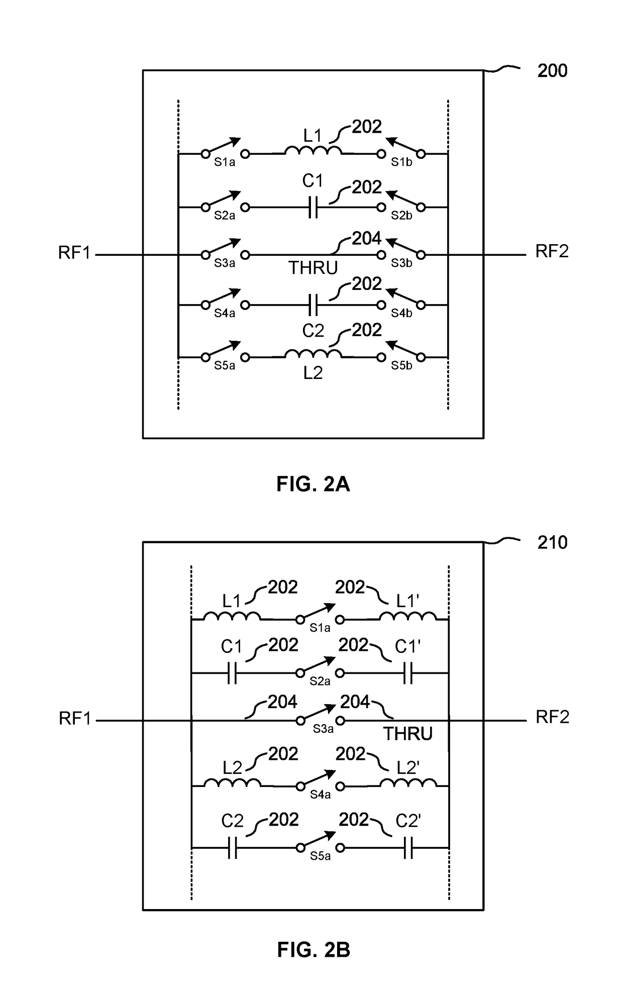
[0024]FIG. 2A is a block diagram of a multi-state phase shifter circuit 200 having low insertion loss and good return loss in accordance with the present invention. The illustrated phase shifter circuit 200 has two ports, RF1, RF2 connected by a plurality of n parallel signal paths each comprising a pair of switches Sna and Snb and an associated phase shift element 202. In the illustrated example, the phase shift elements 202 comprise, for example, one or more inductors Ln, one or more capacitors Cn, or one or more transmission lines, each series connected between corresponding switch pairs Sna-Snb. An optional parallel signal path may comprise a THRU conductor 204 (e.g., a simple wire or IC trace or similar conductor) series connected between corresponding switch pairs Sna-Snb. The illustrated phase shift elements 202 may be physically located on the same integrated circuit (IC) die as the switch pairs Sna-Snb, or an IC may be configured with conductive pads to enable connection of...

second embodiment

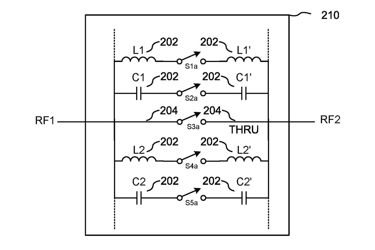
[0028]FIG. 2B is a block diagram of a multi-state phase shifter circuit 210 having low insertion loss and good return loss in accordance with the present invention. In this embodiment, the phase shifter circuit 210 has two ports, RF1, RF2 connected by a plurality of n parallel signal paths each comprising a switch Sna and at least one associated phase shift element 202. In the illustrated example, the phase shift elements 202 comprise, for example, one or more inductors Ln, Ln′, one or more capacitors Cn, Cn′, or one or more transmission lines series connected with a corresponding switch Sna. An optional parallel signal path may comprise a THRU conductor 204 in series with a corresponding switch Sna.

[0029]In each signal path, it would generally be preferred to “split” the phase shift elements 202 as shown—for example, with inductor pairs Ln, Ln′ or capacitor pairs Cn, Cn′ bracketing a switch Sna—so as to provide a “balanced” symmetric circuit with respect to ports RF1 and RF2. In pa...


PUM


Abstract

A multi-state phase shifter circuit having both low insertion loss (IL) and good return loss. Two or more phase shift elements are combined into a single cell architecture to reduce the number of series-connected FET switches and reduce the total IL. One embodiment has two ports connected by parallel signal paths each comprising a pair of switches and a phase shift element comprising, for example, an inductor, a capacitor, a transmission line, or a conductor. Another embodiment has two ports connected by parallel signal paths each comprising a switch and at least one associated phase shift element. The switches in each parallel signal path allow the associated phase shift element to be placed in-circuit under the control of an applied signal. The sets of switches may be independently controlled, so that multiple parallel signal paths may be switched into circuit between the phase shifter circuit ports at the same time.

Description

BACKGROUND[0001](1) Technical Field[0002]This invention relates to electronic radio frequency (RF) circuits, and more particularly to programmable multi-state RF phase shifter circuits.[0003](2) Background[0004]Electronic phase shifter circuits are used to change the transmission phase angle of a signal, and are commonly used to phase shift radio frequency (RF) signals. It is often necessary to change the phase of RF signals for applications such as in-phase discriminators, beam forming networks, power dividers, linearization of power amplifiers, and phased array antennas, to name a few. Modern phase shifter circuits may be digitally controlled and thus provide a discrete set of phase states that are selected by a digital control word.[0005]FIG. 1 is a block diagram of a conventional 3-bit (8 state) binary-weighted, series connected phase shifter 100. The illustrated phase shifter 100 includes three series-connected phase shift cells 102-1 to 102-3, each including a respective induc...

Claims


Application Information

Patent Timeline
IPC IPC(8): H03H7/19
CPCH03H7/19
Inventor GAMAL EL DIN, MOHAMEDSTEHR, UWE
Owner PSEMI CORP
Why Eureka
Try Eureka